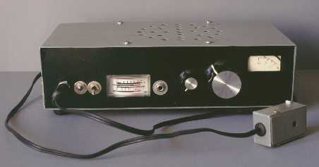
A 40 meter SSB QRP transceiver
 In the ages old Q-code
formerly used in telegraphy communication, "QRP" meant "please reduce power",
or, if followed by a question mark, "should I reduce power?" Well,
Morse code is slowly dying out, even if it is still far from completely
dead. And the Q-code has been adapted to other purposes, misused and abused,
and one such well established misuses is employing the three letters "QRP"
to signify a low power transmitter or transceiver.
In the ages old Q-code
formerly used in telegraphy communication, "QRP" meant "please reduce power",
or, if followed by a question mark, "should I reduce power?" Well,
Morse code is slowly dying out, even if it is still far from completely
dead. And the Q-code has been adapted to other purposes, misused and abused,
and one such well established misuses is employing the three letters "QRP"
to signify a low power transmitter or transceiver.
How low is "QRP"? Some people define it as anything up to 100 Watt,
but the more commonly accepted limit is 10 Watt input to the last stage,
or 5 Watt output. There are many contests in which one has to stay within
5 Watt output to be considered a QRP station. This was one of the reasons
to design the transceiver described on this page for 5 Watt power output.
Another reason was that this power is a good compromise between being heard,
and not needing too much energy, a very important consideration in backpack
portable operation, which was the main purpose of this radio when I designed
it back in 1987.
History
I started building QRP transceivers even before I got my first ham license.
It was simple: There was an age limit in place, so that no one younger
than 15 could get a license. And I was only 13. So, unable to use radios,
nothing kept me from learning to build them. My first project was a direct
conversion 40m receiver with a bipolar wide band preamplifier and a JFET
mixer, copied from a QST article, which was so noisy that it only heard
fairly local stations. I had not yet discovered that component leads could
be cut, so I assembled it keeping the full length leads! The base was a
piece of wood onto which I glued small copper islands. It's just too bad
that I don't have a photo of it! After the first session of criticism
by my elmer, XQ5BIB, Emilio, I disassembled that thing and built a second
version, on very crude printed circuit boards. This time I did cut the
component leads to convenient lengths... And I even added a transmitting
section, the schematic of which I got from XQ5BIB, who had put together
several stages taken from different ARRL publications. It did work, at
1 Watt output on double sideband! I built that radio into a long aluminum
cabinet, covered it with wood-looking vinyl, and proudly showed it to Emilio.
He was the one to try it on the air for the first time. During that test,
suddenly he had one of the knobs in his hand... The set screw wasn't tight
enough. I earned much laughter, but the radio was working!
Following that, in 1982 I built my first radio that included some design
of my own. It was based on another QST article for a CW transceiver, which
I modified for DSB. This radio too was a direct conversion design, and
worked quite well. Then, in 1985, I built a more elaborate version of that
same thing, with higher power. Finally, in 1987 I turned my back to direct
conversion, and designed the radio described here, from scratch. This is
still the crowning of my QRP career. It works very well to this day, has
never had any failure and always attracts crowds when I show it off in
public.
Some photos illustrating this history are on my homo ludens radiactivus
page.
My previous QRP transceivers used to carry just the year as a model
number, so I had the QRP 82, QRP 85, and some others. But the performance
of this new QRP transceiver was so much in another league than all the
previous ones, that I gave it a new model designation: PQD. This
stands for the Spanish phrase primer QRP decente, meaning the
first decent QRP!
The Design
This transceiver was conceived as a power-efficient, small, lighweight
unit to be carried in the backpack, along with antenna and battery, for
use during trekking and mountaineering trips. It had to be reasonably rugged
and reliable, and perform well. Furthermore, I wanted it to solve all the
problems the old DSB transceivers had, such as frequency instability, distorted
modulation, lack of sensitivity and selectivity, and others. The design
that resulted is simple, straightforward and quite conventional, except
for a few simplifications and improvements that set it apart from the most
conventional designs, such as the lack of a microphone preamplifier.
This block diagram shows the basic layout of the radio. You can click
the image to obtain a high resolution version of it, which is a lot better
for printing. If your browser refuses the open the high resolution image,
right-click instead of left-click, choose to save the file, and then open
it with a good image viewing program, such as IrfanView.
Let's start the functional description at the antenna (lower left corner).
The receive signal enters through the TX low pass filter and is 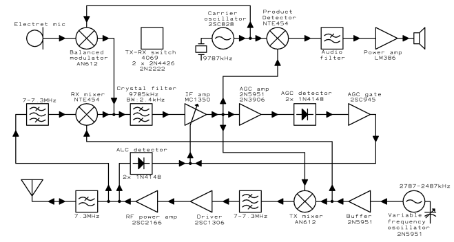 routed
straight to the receiver via passive circuitry. There it passes a band
pass filter tuned to the 40m band, and goes without any preamplification
to a MOSFET mixer. The reasons for both using a MOSFET-based mixer and
not using a preamplifier are routed in the need to get the best possible
ratio between receive capabilities and power consumption. MOSFET mixers
have a high impedance, so their power consumption can be low; and they
need almost no driving power, so there is no need for powerful buffer stages
after the oscillator; and they provide a substantial conversion gain, obviating
the need for a preamplifier! The downsides are more noise and less dynamic
range than some other mixers. But on 40 meters, band noise is so high that
the mixer noise is of no consequence; and not using a preamplifier, the
incoming signals are usually not strong enough to cause overload. Certainly
when out in the wild, there are no strong nearby stations! In large cities
with lots of hams, front end overload can occur, but has not been a problem
for home use of this radio. In any case, for the power consumption limits
I set myself for this radio, the MOSFET mixer offerred the best possible
performance.
routed
straight to the receiver via passive circuitry. There it passes a band
pass filter tuned to the 40m band, and goes without any preamplification
to a MOSFET mixer. The reasons for both using a MOSFET-based mixer and
not using a preamplifier are routed in the need to get the best possible
ratio between receive capabilities and power consumption. MOSFET mixers
have a high impedance, so their power consumption can be low; and they
need almost no driving power, so there is no need for powerful buffer stages
after the oscillator; and they provide a substantial conversion gain, obviating
the need for a preamplifier! The downsides are more noise and less dynamic
range than some other mixers. But on 40 meters, band noise is so high that
the mixer noise is of no consequence; and not using a preamplifier, the
incoming signals are usually not strong enough to cause overload. Certainly
when out in the wild, there are no strong nearby stations! In large cities
with lots of hams, front end overload can occur, but has not been a problem
for home use of this radio. In any case, for the power consumption limits
I set myself for this radio, the MOSFET mixer offerred the best possible
performance.
The VFO runs at a rather low frequency of roughly 2.5 to 2.8 MHz.. This
produces a very high frequency stability. The oscillator uses a JFET, and
a single buffer stage, also employing a JFET. As a result, the entire VFO/buffer
circuit has a very low power consumption, which as an added bonus reduces
any heating that could cause frequency shifts. The VFO uses high stability
polystyrene capacitors and an air-wound coil. The output of the buffer
drives the MOSFET mixer. The output of the mixer goes through a crystal
filter, which has a center frequency near 9.8MHz and a bandwidth of 2.4kHz.
Then comes a gain-controlled IF amplifier in an MC1350 IC, which is the
main gain contributor in this radio, but also the main power consumer!
The output of the IF amp goes to a MOSFET product detector, which gets
its BFO signal from a crystal oscillator and produces audio output, which
after passing the volume control is amplified by an LM386 IC and delivered
to an internal, relatively large loudspeaker, or to external phones.
A sample of the IF signal is further amplified by a JFET and a bipolar
transistor to a rather high level, rectified, and applied through a gate
circuit to the gain control input of the IF amplifier chip. This IF-derived
automatic gain control eliminates the typical bumps and pops so common
of audio-derived AGC, which is used in so many simple transceivers!
For transmission, the audio signal coming from a tiny electret microphone
is directly applied to an IC balanced mixer, which also gets a signal from
the BFO. The resulting double sideband output is applied to the crystal
filter, and the SSB signal that comes out of it is amplified by the
MC1350, then applied to a second balanced mixer, also implemented in an
IC. This second mixer gets the VFO signal, thus producing a SSB output
on the transmit frequency, at a power level of roughly 2 to 3 mW. This
signal is filtered by a band pass circuit, and then amplified to
the 5 Watt output level by just two tuned high gain stages. After
low pass filtering, the RF power reaches the antenna connector.
A sample of the RF voltage in the output stage is rectified and used
for automatic transmit level control. This eliminates the need for a microphone
gain control and maintains proper modulation over a reasonable range of
voice intensities and mike distances, while also affording a moderate amount
of speech compression! Together with a clever shaping of the TX audio response,
this gives the little radio a transmit punch that makes many old-timers
shake their head in disbelief: "This can't be just 5 Watts!"
TX-RX switching is done with electronic switches, using no relay. A
CMOS gate IC and three small transistors take care of this task.
Specifications
You surely want to know how well this radio performs. So, here are the
basic specifications, measured in 1988, when I published this transceiver
in the Chilean RadioAfición magazine:
Frequency coverage:
7.0 to 7.3 MHz
Operation mode:
LSB
Frequency stability:
100 Hz in 30 minutes, worst case
Power supply voltage:
12 V nominal, while 10.5 to 14 V is OK
Current consumption: RX:
30 mA at no output, 33 mA average, 90 mA at max output
TX: 270 mA at no output, 500 mA average,
1 A at max output
Meter readings:
RX signal - TX power - Battery voltage
Sensitivity for 10dB S/N:
1 µV
USB rejection:
50 dB
Image rejection:
60 dB
IF rejection
60 dB
Audio output power:
0.6 W
AGC range:
65 dB
TX output power:
5 W
Mike sensitivity:
50 mV
Carrier suppression:
50 dB
USB suppression:
50 dB
Harmonics suppression:
48 dB
SWR protection:
Infinite
Audio processing:
8 dB compression, high frequency emphasis
Dimensions:
208 x 128 x 61 mm, including all projections
Weight:
0.61 kg
As you can see, the specs are quite attractive for the use intended!
And practical use of this radio over many years confirmed its great usability
and fun!
Circuit design details
I designed this radio during a long summer vacation trip through southern
Chile and Argentina. In the evening hours, or while my parents were sleeping
their siesta, I had time and the necessary inspiring surroundings
to come up with some interesting design details. Some things here are quite
unconventional and deserve close attention.
Here is the schematic diagram. You can click on it to download a high
resolution version for printing. As with all high resolution images on
this web site, if your browser refuses to open it, right-click, save, and
open it with an image viewer.
If you live in the USA, you may be surprised to see resistors drawn
as rectangles instead of zigzag lines. This is the European standard, and
I hope you won't be bothered by it. At the time I designed this radio,
I drew all my schematics in European norm, and even if the schematic shown
here was re-drawn by computer in 2002, I tried to make it look as close
as possible to the hand drawn original of 1987! I did not use a scan of
the original, simply because a hand-drawn and scanned image has an immensely
larger filesize and lower quality than a digitally generated image!
Note that all inductors have their inductance values shown. 3µ2,
for example, means 3.2 µH. When there are taps, their position is
shown in percentage of turns from one side. All values of adjustable inductors
are nominal values, and the inductors should be adjustable over 30% or
so to each side, unless noted otherwise.
Now, let's start in the lower right corner, where the VFO sits.
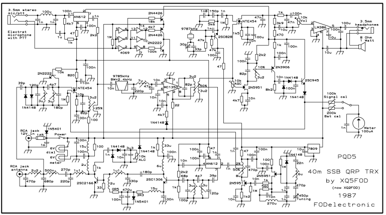 The
VFO is a Colpitts design with Clapp reminiscences. It uses a 450pF (maximum)
variable capacitor taken from an old AM pocket radio. As these variable
capacitors have a nonlinear capacitance to position ratio, I used a series
capacitor to almost fully linearize the response. The oscillator coil is
wound on a former with a small adjustable ferrite core, using enough turns
to barely introduce the core into the coil for the desired inductance.
This reduces any instability caused by the core. The VFO output is amplified
by a tuned JFET buffer, which has two taps on its tank: One delivers several
Volt of RF to the MOSFET RX mixer, while the other delivers a small RF
voltage to the IC TX mixer. The oscillator and buffer are powered from
a three-terminal regulator, which also powers the crystal oscillator, while
everything else runs directly off the 12V supply.
The
VFO is a Colpitts design with Clapp reminiscences. It uses a 450pF (maximum)
variable capacitor taken from an old AM pocket radio. As these variable
capacitors have a nonlinear capacitance to position ratio, I used a series
capacitor to almost fully linearize the response. The oscillator coil is
wound on a former with a small adjustable ferrite core, using enough turns
to barely introduce the core into the coil for the desired inductance.
This reduces any instability caused by the core. The VFO output is amplified
by a tuned JFET buffer, which has two taps on its tank: One delivers several
Volt of RF to the MOSFET RX mixer, while the other delivers a small RF
voltage to the IC TX mixer. The oscillator and buffer are powered from
a three-terminal regulator, which also powers the crystal oscillator, while
everything else runs directly off the 12V supply.
Now let's jump to the lower left side. From the antenna connector, the
signal gets through a low pass filter section and is coupled into a double
tuned circuit, which passes the 7 to 7.3 MHz range and little else.
Two diodes across the first tuned circuit will clamp the high level
RF reaching here during TX. The output of the filter gets to one gate of
the mixer MOSFET, which gets the VFO signal on its other gate. The bipolar
transistor at the output of the filter conducts during TX, thus avoiding
the TX signal leaking through to the following stages. During RX this transistor
is off.
The mixer has its drain permanently powered from 12V, while the
source is grounded during RX and put to 12V during TX. In this way the
mixer is switched off during TX. While receiving, the IF signal appearing
on the drain is filtered by a tuned circuit, and link-coupled into
the crystal filter. As you may know, crystal filters require well defined
input and output load impedances to work well. The turns ratio of the transformer,
together with the 10k resistor across the primary, play a vital role in
this. The circuit's resonance is broad enough to properly terminate the
filter on all frequencies where this is important.
This signal is also applied to the TX mixer's output, but since this
one is off during RX, it does not significantly load that line.
The crystal filter's output is impedance-matched with a PI network to
the IF amplifier. As this IC has a well defined input impedance, it can
be used to load the filter, achieving best efficiency. The differential
output of the IC is converted to a single-ended one in a tuned circuit,
the output of which goes to the product detector. The second gate of this
detector MOSFET gets a signal from a simple crystal beat frequency oscillator,
which can be set to the exact frequency by a small trimmer. The output
of the detector is low-pass filtered to remove any RF signals, and the
resulting audio is fed to the volume control and then to an LM386 amplifier
IC, configured for its minimal gain, which is ample in this case, thanks
to the high conversion gain of the MOSFETs. The 386's output goes to a
headphone connector, which passes it through to the internal speaker when
no headphone is connected. This speaker is a relatively large one - as
large as I could fit in the small box of this radio. I learned early in
my portable operation career that the added weight of large speakers pays
for itself: They are a lot more efficient than small speakers, so less
audio power is needed, which reduces battery drain! 50 more grams in a
speaker can save several hundred grams in additional batteries!
The IF amplifier output is also passed through a trimpot and applied
to a two-stage tuned amplifier, followed by a detector. The resulting AGC
signal is current-amplified by a transistor powered from the 12V RX bus,
which serves several purposes: It switches off this AGC source during TX,
makes the proper fast attack and slow release of the AGC in conjunction
with the 100nF capacitor at the base, and affords quick discharge of this
capacitor during TX, so that a new RX period will not have AGC hangover
from previous reception.
When the operator presses the PTT button, a 4069 CMOS IC will get this
signal, and switch on the 12V TX bus, which was actively held down during
RX. It will also switch off the 12V RX bus. Several things happen at this
point: The RX MOSFET mixer goes into high impedance, the product detector
shuts off, the RX AGC line is interrupted, the RF input to the receiver
is clamped to ground, while power is applied to the electret microphone,
the two TX mixers and the the bias circuit of the TX driver. This sets
the scene for transmission.
Electret microphones are very small, lightweight, inexpensive, and contain
an internal FET that delivers a pretty high output level. This allowed
me to completely skip any further audio amplification, and instead apply
the microphone signal directly to the rather sensitive AN612 doubly balanced
mixer IC. The relatively small coupling capacitor produces a low frequency
rolloff, which is surprisingly effective in making the signal sound larger
than it is! 90% of a voice's power is concentrated in the low frequency,
while 90% of the intelligibility is in the high frequencies. Thus, it's
a really good thing to emphasize the high range, and avoid wasting too
much of our precious power on the useless lows! This radio invariably draws
reports of "extremely crisp, clear, highly intelligible audio"!
It's important not to apply excessive carrier voltage to the mixer IC,
because it will simply block, and deliver no output! The capacitive voltage
divider at the crystal oscillator cares for this task.
The mixer's output is applied to the crystal filter. At this time, the
RX mixer MOSFET is in high impedance, guaranteed by having low voltage
on its gate 1 and 12V on both drain and source! So it will not conduct,
allowing the 10k resistor across its tuned circuit to keep performing its
task of providing a well defined source impedance for the filter, into
which the TX mixer injects its signal through the rather high 2.2k resistor.
The crystal filter selects the lower sideband, as the crystal oscillator
sits a little bit above the filter's passband.
The MC1350 works in TX just like it does in RX, only at a higher signal
level. Its output couples into the second AN612, which gets a low level
carrier signal from the VFO buffer and generates outputs on 7 and
12 MHz, of which the following double tuned bandpass filter selects the
7 MHz one.
The collectors of both the driver and power amplifier transistors are
permanently powered from the 12V line. The bias of the driver is controlled
by the switching circuit. When enabled, the driver transistor is biased
into class A, and its emitter current is used to bias the power amplifier
into class B operation! This is highly power-efficient, and at the same
time allows to switch the entire power amplifier chain with just a few
mA! This is a scheme I invented, and I was mighty proud of it at the time.
Years later I have seen it in use by other designers, who probably came
up with it independently of myself. It's just such a logical thing to do!
A small note about the 1N5401 bias diode: This is a 3 Ampere diode,
but don't be tempted into replacing it by a smaller one! It has to conduct
much less than one Ampere, but it is still necessary to use the big diode,
because smaller ones have a slightly larger voltage drop, and will over-bias
the power transistor, making it run at low efficiency or even burning it
out by thermal runaway! Don't even replace this diode by one rated at higher
voltage, such as the 1N5408, because this one also has a higher voltage
drop!
Otherwise these two stages are pretty straightforward. The band pass
filter is impedance matched to the driver transistor's base, while L-C-C
networks do the interstage matching and the power amplifier collector matching.
The transistors are intended for 27 MHz operation, and at 7 MHz they are
quite "hot", delivering high gain but also loving to self-oscillate. Good
construction practices are essential for achieving stability when putting
this much gain into just two RF stages which are tuned at all ends!
A simple RF rectifier samples to collector RF voltage of the power transistor,
and produces an ALC voltage from it, fed into the IF amplifier. This achieves
automatic transmit level control, and the time constant was selected such
as to provide a moderate level of speech compression. As a byproduct, this
circuit limits the output during high SWR conditions. The trimpot is set
to obtain 5W output power.
The power supply is routed through a fuse and clamped by a reverse-connected
diode. In case of applying the wrong polarity, the fuse will open, avoiding
further damage. Then comes the power switch, linked with the volume control.
A separate toggle switch allows to power two little lamps that light the
dial and the meter. During normal battery operation these lamps are left
off, since they drain several times as much current as the entire radio
in RX operation!
The meter is normally connected to the AGC/ALC line, but can be switched
over to the 12V bus. In both positions there are trimpots to properly calibrate
meter response.
Mechanical construction
 The entire radio
is built on a single printed circuit board. This concept is applied to
such an extent, that not only the connectors and the meter are mounted
on the board, but even the dial reduction drive mechanism is!
The entire radio
is built on a single printed circuit board. This concept is applied to
such an extent, that not only the connectors and the meter are mounted
on the board, but even the dial reduction drive mechanism is!
A frame made from 1mm thick aluminum sheet runs around the printed circuit
board, forming the front and rear panels, and the internal sides. Two almost
symmetrical U-shaped pieces of the same material form the top and bottom
covers while also doubling the sides. This allows very easy access to both
the component and solder sides of the board. The speaker is glued to the
top cover, which is properly drilled to let the sound pass.
The printed circuit board measures 20 x 10 cm, and is double sided.
The top side is left mostly intact, to serve as ground plane, except only
in the VFO area, where the top side was etched away, in order to avoid
unstable parasitic capacitances which could affect frequency stability.
All ground connections are soldered on the top side, which is made easy
by the relatively low population density of the board. Some parts, like
the IF transformers, have to be mounted a bit off the board to allow soldering
under them. All holes which are not ground connections had their top side
copper cleared away around them, using a 3mm drill bit.
A plated-through board would of course avoid the need for top side
soldering, but I didn't have the technology back then to make one! The
board was made using my home methods of the time: I designed it with a
graphite pencil on plain paper, then clamped a transparent foil onto the
design, applied rub-on pads, then made the traces using self-adhesive black
tape of different widths. This original was then photographically copied
onto the board, using Kontakt-Chemie Positiv-20 spray, and then the board
was etched.
 The result
is what you can see here! The etching quality was quite good, even if the
layout does not look as clean and computerish as a modern software-generated
one. But for RF use, these softly curved tracks are actually better than
the sharp bends most PCB software makes!
The result
is what you can see here! The etching quality was quite good, even if the
layout does not look as clean and computerish as a modern software-generated
one. But for RF use, these softly curved tracks are actually better than
the sharp bends most PCB software makes!
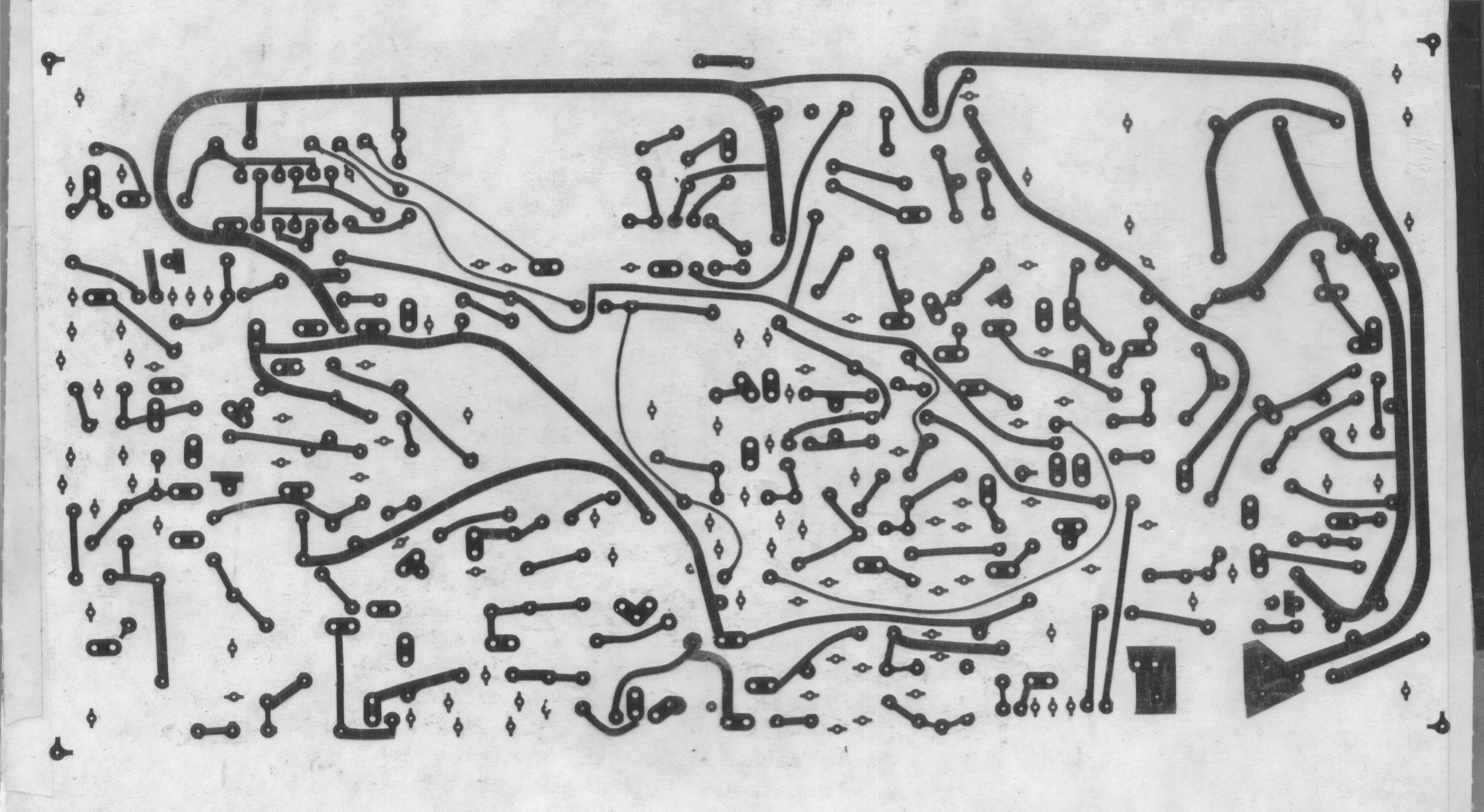
I made a high resolution scan of the original
PCB layout. It will probably not be usable as a mask to directly make
a PCB, but should be useful as a base on which to do a digital edit for
generating a workable mask.
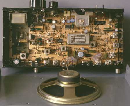
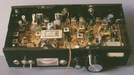
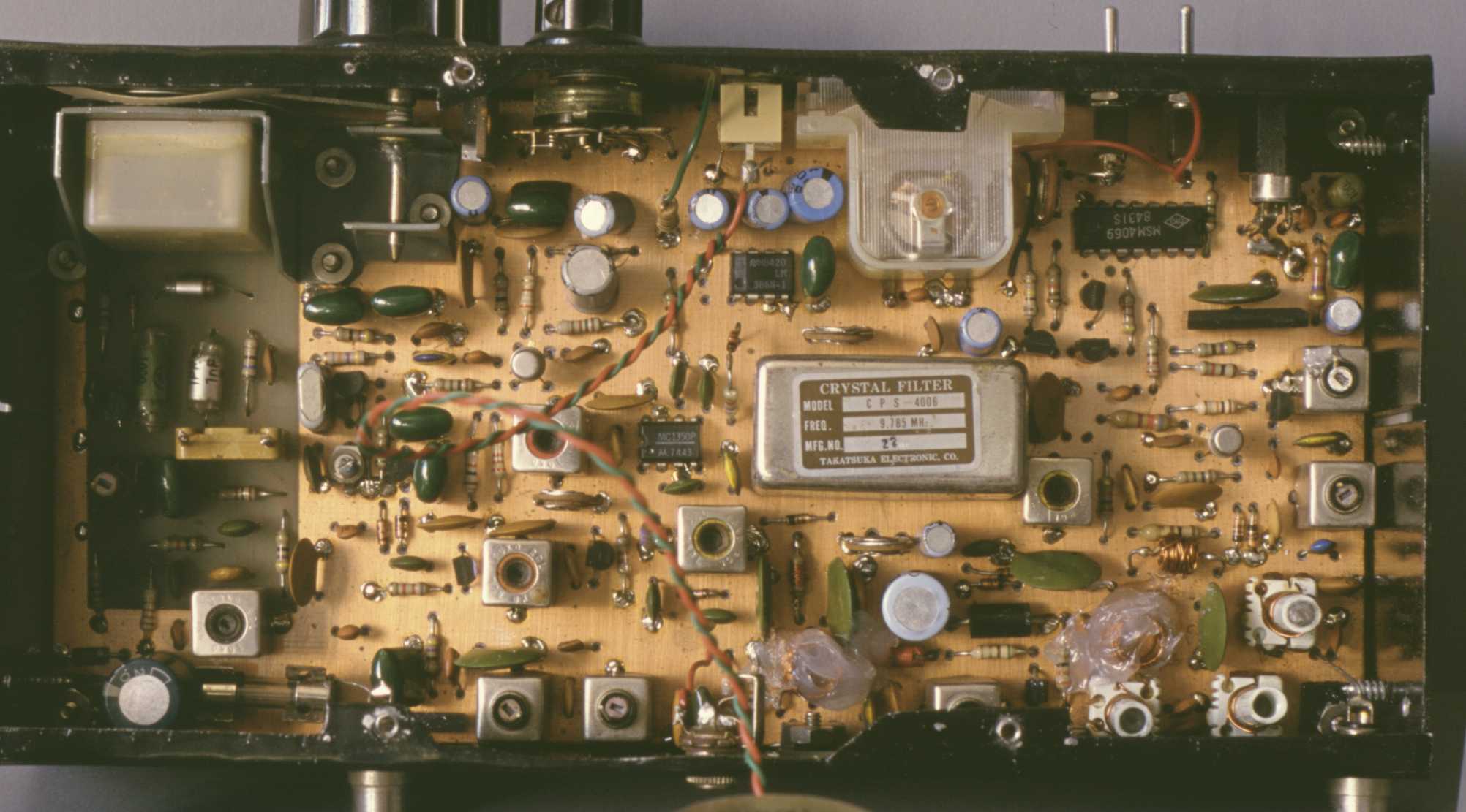
I did never make a component location diagram, but instead I made a
high
resolution photo of the radio's inside. You can use this photo to find
out which part goes where, if you copy this design!
The unsoldered pins are those ground connections that are soldered on
the top side. Note the three jumpers: The red one is a 12V line, while
the other two are oscillator signal connections, made with small shielded
wire. There are no jumpers on the top side.
The 100 Ohm resistor was originally intended to serve as winding core
for the decoupling choke of the power amplifier stage, but later I found
it better to wind this choke with a larger diameter, and so I mounted the
resistor on the bottom side.
The spacing between the PCB and the bottom plate is barely 5 mm.
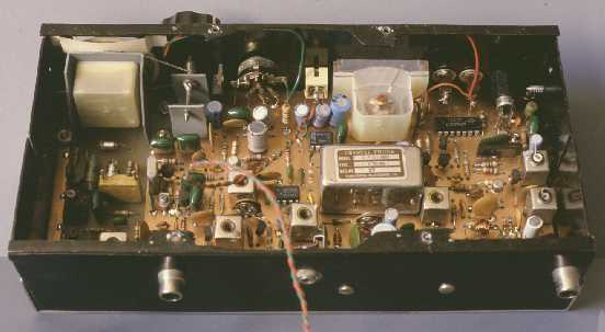
 Here's another
view of the radio's inside, exposing the otherwise hidden components along
the rear panel, among which the TX power amplifier chain is prominent.
Here's another
view of the radio's inside, exposing the otherwise hidden components along
the rear panel, among which the TX power amplifier chain is prominent.
At this time you may be asking where I found all those special components,
like the crystal filter. Well, it's quite simple: The early 1980's brought
a rush of Citizen's Band activity, and by 1987 the rush was ending. There
was a surplus of CB radios, so if a CB radio failed, the likelihood for
the owner to send it in for repair was small. During the early design stages
of this radio I asked around, and was given an old Royce 639 transceiver,
which had a burned PLL chip and thus could not be repaired cheaply. PLL
chips were not easily available here. I took that Royce apart, and used
the crystal filter, BFO crystal, signal meter, coil forms, and many other
parts from it!
 Here is yet
another view, that allows you to peek at the back side of the front panel.
The volume control potentiometer I found was not intended for PCB mounting.
So I simply wired it to the board, just like the connectors and switches.
Here is yet
another view, that allows you to peek at the back side of the front panel.
The volume control potentiometer I found was not intended for PCB mounting.
So I simply wired it to the board, just like the connectors and switches.
Note the wiring of the illumination system. Actually, there is a resistor
in series with the two tiny bulbs, and this resistor is not in the schematic...
I could not find 6V bulbs, so I had to use 5V ones!
You may have noticed that I used RCA connectors for both the 12V supply
and the antenna, which may look like a dangerous situation. But it is not!
If you mix up the cables and connect 12V to the antenna input, nothing
will happens, since it is DC-blocked. RCA connectors behave quite well
at RF, are much lighter and smaller than common coax connectors, and also
can easily carry the 1 Ampere of supply current needed by this radio. The
only true disadvantage is that a male RCA carrying 12V power poses a short-circuit
hazard. But I had standardized on RCA connectors for all low current 12V
needs in my shack in times when I still didn't think much about safety,
so I didn't want change this standard. In fact, to this day I still use
RCAs for all small 12V connections, and simply use care to avoid shorting
them.
The 3.5mm connector in the middle of the back panel is not on the schematic.
It is simply an output of the 12V TX line. I used that output to switch
an external linear amplifier for QRO operation at home. The first amplifier
I built was a broadband push-pull design, using two CB transistors and
delivering about 30 Watt. Then I built the big one, which used two 6146B
tubes in parallel, powered from slightly over a kilovolt, running at a
300 Watt input level! By the way, that one was my first tube project.
But what will probably most catch your attention is the tuning mechanism.
I made a detail scan of that area of this photo, to better show it - because
it's really worthwhile to see! :-)
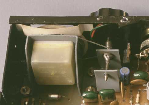 The gray piece
is a bracket specially crafted from 1mm aluminum sheet, that holds both
the variable capacitor and the tuning axle. And the tuning axle is, well,
nothing else than a discarded Parker ballpen refill! The thick part of
it has the right diameter to carry the large tuning knob, while its tip
is nicely thin so that it will have precise guiding and low friction, while
also allowing a great reduction ratio between the tuning knob and the variable
capacitor. It is hollow, saving some weight, and made of high quality steel.
And it was free!
The gray piece
is a bracket specially crafted from 1mm aluminum sheet, that holds both
the variable capacitor and the tuning axle. And the tuning axle is, well,
nothing else than a discarded Parker ballpen refill! The thick part of
it has the right diameter to carry the large tuning knob, while its tip
is nicely thin so that it will have precise guiding and low friction, while
also allowing a great reduction ratio between the tuning knob and the variable
capacitor. It is hollow, saving some weight, and made of high quality steel.
And it was free!
The ballpen refill was simply cut to the proper length, inserted in
the bracket, and two washers were soldered to it, in order to keep it in
place. The original pulley of the old AM radio was kept on the variable
capacitor, a cord was strung around to complete the reduction drive of
about 9:1. The capacitor tunes from 7 to 7.3 MHz over about
120 degrees, so this gives about 100kHz per revolution of the tuning knob.
This is quite fast for older gents, but I never had trouble precisely tuning
in a station. It is millimeter work, in any case, but perfectly possible
to do quickly.
The dial was made of stiff paper, and calibrated by measuring the frequency
on a frequency counter. The markings were made with a graphite pencil,
which is a lot more permanent than ink pens of any kind! The dial was glued
to the pulley, and another piece of paper was glued in as a backplane,
to keep people from looking into the radio through the dial opening! The
small bulb was glued to the front panel in such a position as to evenly
illuminate the portion of the dial visible through the front panel cutout.
A small piece of clipped resistor lead serves as a pointer. On the dial,
10kHz markings are only about 1 mm apart, but still the dial is precise
enough to get within 2kHz or so of any given frequency - close enough to
find your buddy or a net!
Using this radio
After building this transceiver in 1987, and until 1992, it was my main
HF radio for both home and portable use. After that date, I was given an
old Heathkit TX-RX combo, and shortly later bought a shining new Kenwood
TS450S-AT! This relegated the QRP transceiver to portable backpack use,
which would simply be absurd to attempt with commercial radios requiring
a car battery to run... At home, occasionally I still put the QRP transceiver
on the air, just for fun, but not very often.
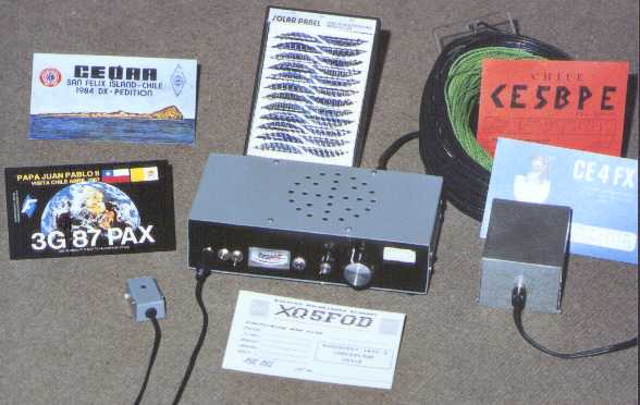 Over the first
months I made a lot of interesting contacts. This photo was made for the
1988 publication in RadioAfición, showing a colorful sampling of
QSL cards earned with this radio: A contact with a DXpedition on the highly
wanted San Felix Island, the card of a special event station that followed
Pope John Paul II during his 1987 visit to Chile, and some less special
QSL cards, including my own instead of a signature... The other items in
the photo are all that's needed for a complete backpack HF SSB station:
The radio, the tiny microphone, a battery box with 10 NiCd cells of 1.2
Ah capacity (with modern cells that box would be a lot smaller!), a small
solar panel to charge the battery, and the antenna: This antenna
is a full size dipole made from thin, flexible AC power wire, fed by RG174
miniature coax cable. This cable saves a lot of weight and causes less
than 1dB loss on 40m. Three pieces of 3mm nylon rope, of three different
lengths, are included in the roll. This allows to quickly raise the dipole,
using any tree, post, mast, roof, or whatever as a support.
Over the first
months I made a lot of interesting contacts. This photo was made for the
1988 publication in RadioAfición, showing a colorful sampling of
QSL cards earned with this radio: A contact with a DXpedition on the highly
wanted San Felix Island, the card of a special event station that followed
Pope John Paul II during his 1987 visit to Chile, and some less special
QSL cards, including my own instead of a signature... The other items in
the photo are all that's needed for a complete backpack HF SSB station:
The radio, the tiny microphone, a battery box with 10 NiCd cells of 1.2
Ah capacity (with modern cells that box would be a lot smaller!), a small
solar panel to charge the battery, and the antenna: This antenna
is a full size dipole made from thin, flexible AC power wire, fed by RG174
miniature coax cable. This cable saves a lot of weight and causes less
than 1dB loss on 40m. Three pieces of 3mm nylon rope, of three different
lengths, are included in the roll. This allows to quickly raise the dipole,
using any tree, post, mast, roof, or whatever as a support.
Forget about loaded whip antennas for QRP use! Such antennas have a
low efficiency, and an inefficient antenna fed by low power is an excellent
recipe to not be heard! But with the full size dipole in a decent
location, this radio generates surprising signal reports! I often got reports
of 5-9 +20 from places 500 km away, and usually these reports came paired
with comments about the beautiful, crisp and clear audio!
Is it for you?
If you read this page down to here, then maybe you are considering building
such a radio. If you want to build an exact copy of my radio, the problem
is that you will have to find the special parts: The crystal filter and
its carrier crystal, and the variable capacitor are potentially the most
troublesome parts to get. If you want to make an exact copy, you also will
need a meter that fits the room left for it on the PCB.
I know of roughly 10 people who built this radio after I published it
in RadioAfición. Some of them also gutted a Royce 639, like I did,
to use the parts. Others modified the details, for example by using a crystal
ladder filter made from widely available 10 MHz microprocessor crystals.
Whatever you decide, exact copy or rough copy, you should first find out
if you can get the parts you need. Miniature plastic variable capacitors
are to be found in many hams' junk boxes, but are not easy to buy new nowadays!
Also I don't know if the AN612 ICs can still be found. So, shop around
before deciding!
Back to homo ludens electronicus.
 routed
straight to the receiver via passive circuitry. There it passes a band
pass filter tuned to the 40m band, and goes without any preamplification
to a MOSFET mixer. The reasons for both using a MOSFET-based mixer and
not using a preamplifier are routed in the need to get the best possible
ratio between receive capabilities and power consumption. MOSFET mixers
have a high impedance, so their power consumption can be low; and they
need almost no driving power, so there is no need for powerful buffer stages
after the oscillator; and they provide a substantial conversion gain, obviating
the need for a preamplifier! The downsides are more noise and less dynamic
range than some other mixers. But on 40 meters, band noise is so high that
the mixer noise is of no consequence; and not using a preamplifier, the
incoming signals are usually not strong enough to cause overload. Certainly
when out in the wild, there are no strong nearby stations! In large cities
with lots of hams, front end overload can occur, but has not been a problem
for home use of this radio. In any case, for the power consumption limits
I set myself for this radio, the MOSFET mixer offerred the best possible
performance.
routed
straight to the receiver via passive circuitry. There it passes a band
pass filter tuned to the 40m band, and goes without any preamplification
to a MOSFET mixer. The reasons for both using a MOSFET-based mixer and
not using a preamplifier are routed in the need to get the best possible
ratio between receive capabilities and power consumption. MOSFET mixers
have a high impedance, so their power consumption can be low; and they
need almost no driving power, so there is no need for powerful buffer stages
after the oscillator; and they provide a substantial conversion gain, obviating
the need for a preamplifier! The downsides are more noise and less dynamic
range than some other mixers. But on 40 meters, band noise is so high that
the mixer noise is of no consequence; and not using a preamplifier, the
incoming signals are usually not strong enough to cause overload. Certainly
when out in the wild, there are no strong nearby stations! In large cities
with lots of hams, front end overload can occur, but has not been a problem
for home use of this radio. In any case, for the power consumption limits
I set myself for this radio, the MOSFET mixer offerred the best possible
performance.
