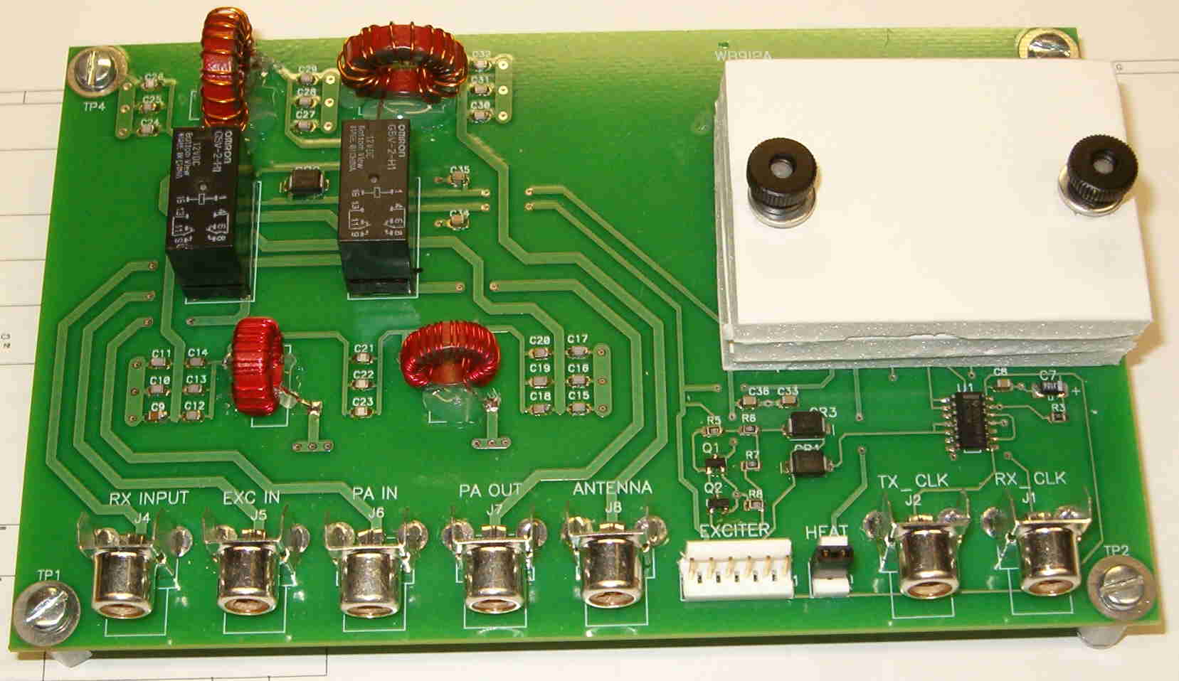
Oscillator-Filter Module
Schematics
PCB Layout
Features
The oscillator-filter module is responsible for generating the RX_CLOCK and TX_CLOCK signals for use by the receiver and exciter modules, providing RF bandpass and low pass filtering for both receive and transmit functions, as well as antenna switching. As designed, this module provides for operation of the transceiver on a single, crystal controlled channel within the 60 meter allocation. Modification for use on other frequencies would be possible. A temperature stabilized crystal oscillator circuit is used for frequency generation to ensure frequency stability over a wide range of temperatures.
Specifications
DC supply voltages: 10 – 15 VDC and 4.5 – 5.5 VDC (regulated)
Operating Temperature: 0 – 70 C
Output levels TX_CLK and RX_CLK: 5 volt CMOS logic compatible
Output frequency: 21.614 MHz (4 x operating frequency)
Frequency stability over temperature: +/- 10 ppm
PCB dimensions: 3.9 x 6.25”
Theory
The PCB layout can be seen here.
U1A forms a pierce crystal oscillator which generates a clock signal at 4x the operating frequency. The clock signal is then sent to U1C and U1D, where it is buffered and gated to either the exciter via J2 (TX_CLK) or J1 (RX_CLK), depending on the logic level of the /REGEN_PTT.
Since the transceiver was intended to be operated in mobile, portable and home environments, it was felt that some sort of temperature stabilizing scheme should be included to keep the transceiver as close to the assigned frequency as possible over the expected environmental temperature range. During the winters, outside temperatures routinely drop below 0 C (32 F) and exceed 32 C (90 F) in the summer. While FCC 97.303 makes no reference to any frequency accuracy specification, it was simply felt that good operating practice would encourage keeping to the assigned frequency as closely as possible, without the use of “heroic” measures.
The stabilization scheme chosen was to simply scatter Positive Temperature Coefficient (PTC) thermistors around the oscillator section, as well as bonding one to the crystal. PTC thermistors behave like normal resistors in that they dissipate power (heat) in response to current passing through them.
PTC thermistors exhibit a unique behaviour, in that their resistance increases as the temperature increases. This temperature to resistance relationship is very non-linear; in fact, the change becomes very rapid above a temperature known as the Transition Temperature. This property can be exploited to make a very simple, self-regulating heater. When the device is below the transition temperature and voltage is applied, heat is dissipated in the device. Heat is conducted out of the thermistor and into the circuit board where it heats the board and nearby components. When the thermistor reaches the transition temperature, its resistance rapidly increases, lowering the power dissipated in the device. This action causes the thermistor to act as a heat source whose temperature is maintained at a nearly constant temperature near the transition temperature. Since heat is being conducted out of the thermistor and into the circuit board, nearby components are held at relatively stable operating temperatures, despite varying environmental temperatures.
The thermistors used in this design were chosen to have a transition temperature of 65 C. Approximately 2 Watts of power (at a supply voltage of 12 VDC) can be dissipated in the thermistors while below the transition temperature. This power drops considerably after the temperature has stabilized.
In order to increase the effectiveness of the thermistors, slots were cut in the PCB material to thermally isolate the oscillator section from the rest of the board. A small enclosure was built around the oscillator section to further thermally isolate the oscillator from the environment. The enclosure was built from layers of foam board. Foam board consists of a sheet of some type of foam (Styrofoam?) with heavy paper bonded to the outer surfaces. The material is available from art supply stores. Squares of the material were cut, removing material that would interfere with the components, and layers built up until the entire oscillator section was contained. An additional piece was made to cover the bottom of the oscillator. The layers of foam were pressfit over #6 nylon hex spacers to hold them in place.
If the transceiver will be operated in a benign environment where the temperature will be somewhat constant, the heaters may not be necessary. The heaters may be controlled by placing a jumper or switch across J9. Shorting J9 turns the heaters on while an open circuit at J9 turns them off. Not using the heaters will result in a substantial power savings, an important consideration when operating from battery power.
During the course of debugging of the oscillator, a change was made to the original trimming capacitor configuration. The original configuration had C2 populated with a 7-50 pF surface mount trimmer and C1 not populated. It was noted that while this configuration did function as intended, it was difficult to accurately set the frequency with C2. In the end, both C1 and C2 were removed, and a 3 – 13 pF ceramic trimmer from the junk box was added across Y1. This configuration seems to provide enough frequency range to adjust the frequency as needed, while not being overly touchy.
Another (surprising) property that was discovered during debugging was the degree of frequency sensitivity due a change in supply voltage. Varying the supply voltage from 4 to 5 volts would cause approximately 200 Hz shift in oscillator frequency. 200 Hz for a 1 volt change in supply voltage was somewhat more than was expected. This sensitivity to supply voltage is not a problem in this design as the oscillator receives regulated +5V from the exciter module, but, should be kept in mind for future designs.
When the transceiver is in the receive mode, /REGEN_PTT is logic high. This causes transistor Q2 to conduct, which drives transistor Q1 into cutoff (no conduction), leaving relays RL1 and RL2 in their relaxed state. CR2 is a clamping diode which prevents inductive kick from destroying Q1.
RF from the antenna enters J8 (ANTENNA) and passes through a halfwave lowpass filter consisting of L4, L3 and their associated capacitors, to RL2, pins 13 and 4. The signal exits RL2 via pins 6 and 11, where it then enters RL1 at pin 11. The signal passes through RL1 and exits at pin 13, where it then enters a bandpass filter consisting of L2, L1 and associated capacitors. The filtered RF signal leaves the bandpass filter and comes to RL1, pin 4. The signal exits RL1 at pin 6 and leaves the board via J4 (RX INPUT) for use by the receiver module.
When the transceiver is in the transmit mode, /REGEN_PTT is logic low. This causes transistor Q2 to be in a cutoff condition, driving transistor Q1 into saturation (maximum conduction), causing relays RL2 and RL1 to pull in.
RF from the exciter module enters the board at J5 (EXCITER OUTPUT) and enters RL1 at pin 8. The signal passes through RL1 and exits via pin 4, where it then travels to the bandpass filter, consisting of L1, L2 and associated capacitors. The filtered signals returns to RL1 at pin 13, exits at pin 9 and leaves the board at J6 (PA INPUT).
After leaving the board, the signal enters the RFPA module and is amplified to a usable power level. The amplified signal returns to the board via J7 (PA OUTPUT) and is applied RL2, pins 8 and 9. The signal exits RL2 at pins 4 and 13, and is sent to the halfwave lowpass filter consisting of L3, L4 and associated capacitors. After being lowpass filtered, the signal leaves the board via J8 (ANTENNA) where it is ready to be connected to the external antenna.
For those interested, the calculations for the bandpass filter and the halfwave lowpass filter are available. Click here for an Excel spreadsheetwhich calculates component values for the Bandpass filter. The spreadsheet can be saved to the user’s computer and used to calculate component values for two-resonator filters of other frequencies, if desired. Click here for an explanation of the lowpass filter calculations. Please keep in mind these calculations show ideal values; the values used in the final circuit represent combinations of commercially available values that approximate the ideal values.
A simulation of the bandpass filter frequency response can be found here.
A simulation of the halfwave lowpass filter frequency response can be found here.
It should be noted that the outcomes of these simulations are calculations based only on the component values used in the simulation. The simulations do not consider the effects of parasitic resctances and resistances that may appear in the circuit. These parasitics may be attributable to the use of real-world (non-perfect) components and the PCB layout. During debugging of the board, frequency sweeps of the actual circuits showed similar to those depicted by the simulations in the frequency range below 100 MHz. Above 100 MHz, the filter attenuation decreases to values considerably less than those predicted by the simulation. Present thinking is that there is leakage around the filters through the PCB groundplane, or around relays RL1 and RL2, causing the loss of attenuation at the higher frequencies. Plots of the actual responses will be made available when possible.
Bill of Materials
The Bill of Material (BOM) is provided in three different formats. Excel format is ready for use directly in Microsoft Excel. HTML format can be viewed directly on the screen if you do not have Excel or other spreadsheet software. CSV format can be used by most spreadsheet software, including Microsoft Excel and others. Here is an explanation of the columns:
Column Label Meaning
A NI? NI = Component not installed
B Pattern Name This is the name of the component pattern used by the layout software
C Ref Des Component reference designator
D Device Component type
E Val Component value
F Wat Component rating in Watts (if applicable)
G PCT Component tolerance
H Volt Component Voltage rating
I PMFR Primary manufacturer
J PMFR P/N Primary manufacturer part number
K P Vendor Primary Vendor (Note: digi = Digikey)
L P Vendor P/N Part number used by the primary vendor
M SMFR Secondary manufacturer
N SMFR P/N Secondary manufacturer part number
O S Vendor Secondary Vendor
P S Vendor P/N Secondary P/N
Important note:
The listing of any vendor or manufacturer in this Bill of Materials does not in any way constitute any endorsement of any vendor or manufacturer. Vendors, manufacturers and their part numbers are listed soley for convenience of the builder. The information presented in this Bill of Materials may contain errors; the author assumes no liability for the accuracy of the information contained herein. The user assumes all liability for the use of any information presented in this Bill of Materials.
More pictures
Click here for a closeup of the oscillator section.
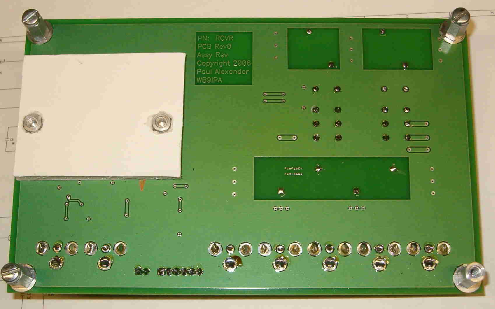
Click here to see the back side of the board.