Exciter Module
Schematics
Sheet 1 Sheet 2 Sheet 3 Sheet 4
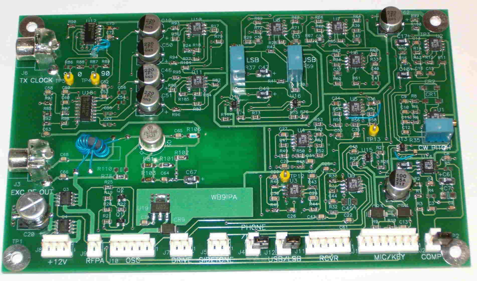
PCB Layout
Features
The exciter module generates Single Sideband Suppressed Carrier and Continuous Wave signals by means of an image-reject modulator, also known as the “phasing method”. The exciter audio path provides for amplitude compression as well as aggressive bandpass filtering of the input audio signal to meet the bandwidth requirements for operation in the 60 meter band.
Specifications
DC supply input: 10 – 15 VDC
Operating temperature: 0 – 70 C
RF output level: +10 dBm PEP
Operating frequency range: 1.5 – 30 MHz
Modes of operation: CW, USB and LSB
Carrier suppression: 30 dB min.
Unwanted sideband suppression: 30 dB min.
PCB dimensions: 3.9 x 6.25”
Theory
The PCB layout can be seen here.
Microphone audio enters the module through connector J1. A maximum of 17 mA bias for amplified dynamic, electret or carbon microphones is provided by R1, R2 and C1. Amplitude compression of the microphone audio signal is provided by U14, an Analog Devices SSM2165. The amount of compression applied to the audio signal is controlled by means of a switch or variable resistor connected to J2. See the SSM2165 datasheet for further details.
U1A forms a phase shift oscillator, which supplies a 700 Hz square wave for use in generation of the CW mode signal. Variable resistor R35 provides for slight adjustment of the oscillator frequency. The square wave is gated (keyed) by means of solidstate switch, U13. Diodes CR3 and CR4 and their associated circuits provide ESD and EMC protection of the keying signal before it is applied to U13. The keyed 700 Hz tone is buffered and lowpass filtered by the circuitry surrounding U2.
DC power (12 volts nominal) enters the PCB through connector J8 and then passes through MOSFET Q4, which provides reverse polarity protection. A MOSFET was chosen for polarity protection because it provides less voltage drop than a series diode, and, in the case of reverse polarity being applied, does not result in a blown fuse, as would a reverse-biased parallel diode. The polarity protected +12 V is applied to the PTT circuitry as well as regulator U19. U19 provides +5 volts for various circuits in the exciter.
Q1 and Q2 form a circuit that regenerates the PTT signal for use throughout the entire transceiver. This ensures that all parts of the transceiver switch between transmit and receive modes at the same time. Q3 switches supplies +12 V to amplifier Q5 while in the transmit mode.
CW or SSB mode audio is selected by solidstate switch U15. The selected audio signal passes to U9A where it is amplified for use in the transmit audio chain, and to U9B for use as transmit sidetone.
U3 forms a 4 pole, highpass filter, while U4 and U5 form 8 poles of lowpass filtering. The audio filtering of this exciter was specifically designed to meet the bandwidth requirements of the 60 Meter band. Part 97.303, which authorizes the use of the 60 Meter band, specifies the use of upper sideband, with a signal bandwidth of not more than 2.8 KHz. Unfortunately, part 97.303 does not go into great detail as to how to determine signal bandwidth. From other FCC requirements, we can infer that the bandwidth of the signal is to be measured at the points where the signal is 25 dB down from the peak amplitude.
If we assume that we will set our carrier frequency 1.5 KHz below the assigned channel frequency and that our signal is to be centered about the channel frequency, we can deduce that our lower audio frequency (at the –25 dB point) will be:
1.5 KHz – (2.8 KHz / 2) = 100 Hz
Similar reasoning can be applied to determine the upper cutoff frequency of the audio chain.
1.5 KHz + (2.8 KHz / 2) = 2.9 KHz
If we were to simply specify a 100 Hz highpass filter followed by a 2.9 KHz lowpass filter, both would require impractically steep (brickwall) rolloff rates.
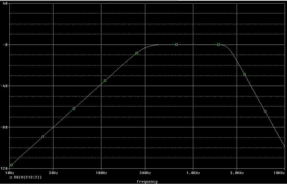
In practice, this filter was realized by the use of a four pole highpass filter with a design cutoff frequency of 300 Hz and a Tchebychev response, followed by an eight pole lowpass filter with a design cutoff frequency of 2400 Hz and a Tchebychev response. The actual response of the filter is –48 dB at 100 Hz and –32 dB at 2900 Hz, ensuring that the bandwidth requirements are easily met, along with some allowance for component tolerances.
The filter was designed by using Texas Instruments’ Filter
Pro software which is available as a free
download from the TI website. A
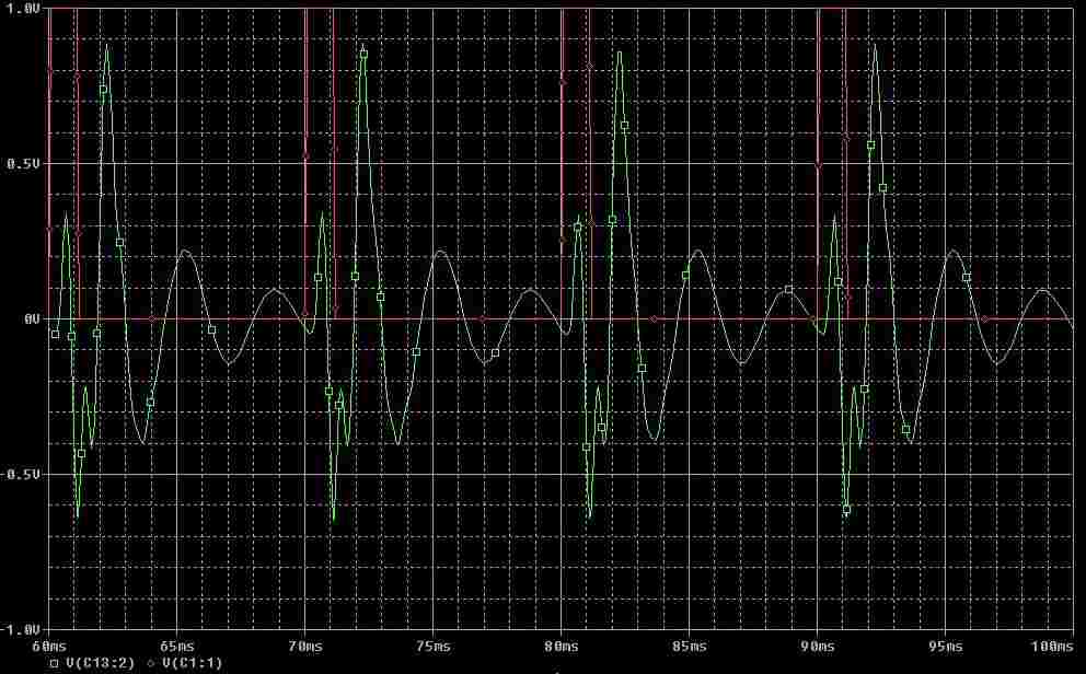
simulation of the filter’s pulse response can be seen here. As can be expected from a filter like this, a large amount of
ringing is evident. A simulation of the
filter’s frequency response can be seen here.
More information concerning the regulatory aspect of the audio filter chain, see the Doug T Smith Editorial Services website as well as FCC 97.303.
The exciter audio phase shift circuit consists of a six-section allpass filter, with three sections in each leg. FILTERED_TX_AUDIO arrives from the audio low pass filter U5B and is applied to both the upper and lower legs of the phase shift circuit. The audio signal passes through the two legs of the phase shift and emerges out the other end with a phase difference of approximately 90 degrees between the two legs. The phase shift circuits were designed with the aid of the J-TEK Allpass Filter Designer to cover the frequency range of 200 to 4000 Hz. All capacitors were chosen to be 0.027 uF, a value that could be obtained in a 0805 SMT package, +/-2% tolerance and with a PPS dielectric. All resistors used in the phase shift circuits are 0805 SMT metal film units with +/-1% resistance tolerance. The phase shifter in the exciter was designed to the same parameters as that in the receiver, allowing use of common resistor and capacitor values in both designs. The J-TEK Allpass Filter Designer is available as a free download.
The phase-shifted audio from the lower chain is applied to two voltage dividers, one divider consisting of R73 and R75, the other consisting of R76 and R74. Audio from the upper chain is applied to another pair of variable voltage dividers consisting of R41, R37 and R38 and another consisting of R70, R59 and R42. R37 and R59 are made variable to allow balancing the audio signal levels from the upper and lower signal chains, in order to obtain the best opposite sideband suppression possible.
Sideband switching is accomplished by means of solidstate switches U16 and U17. These devices are connected as a double pole double throw (DPDT) switch, which selects the application of the upper and lower phase shift chain signal to the TX_I_AUDIO or TX_Q_AUDIO signals, based on the logic level of the USB/LSB line. When the USB/LSB line is at logic low, audio from the upper chain is sent to TX_I_AUDIO and audio from the lower chain is sent to TX_Q_AUDIO. The assignments reverse when the USB/LSB signal is logic high. The USB/LSB signal is controlled by applying a ground or open from an external source (such as a front panel switch). This signal is compatible with 5-volt logic levels to allow control via a microprocessor port.
Now that the transmit audio has been broken into In-phase (TX_I_AUDIO) and Quadrature (TX_Q_AUDIO) components, the two signals arrive at U10 and U11 where inverted and non-inverted versions of each are made. TX_I_AUDIO passes through U10A, which is configured as non-inverting, gain of one, buffer amplifier. TX_I_AUDIO also passes through U10B, which is configured as a gain of one, inverting amplifier. TX_Q_AUDIO passes through an identical circuit. The result is that we now have four audio signals, each separated in phase by 90 degrees. The signals are:
Non-inverted TX_I_AUDIO 0*
Inverted TX_I_AUDIO 180*
Non-inverted TX_Q_AUDIO 90*
Inverted TX_Q_AUDIO 270*
These four phases of the audio signal are passed to U18, which is a Quadrature Sampling Detector (QSD), also known as a Tayloe Detector, operating in reverse. U18 is an SN74CBT3253D, dual, single pole, four position, solidstate switch. To reduce resistive losses in the switch, sections 1 and 2 have been paralleled. U18 passes each of the four audio signals through in a sequence determined by the logic levels seen at U18 pins 2 and 14. The relationship between logic levels and audio signal selected is shown below:
S1 S0 Signal Phase
0 0 INV_TX_Q_AUDIO 270
1 1 INV_TX_I_AUDIO 180
1 0 TX_Q_AUDIO 90
0 1 TX_I_AUDIO 0
The logic sequence at S0 and S1 is provided by U12, a 74AC74 dual D-type flip flop, wired as a divide-by-four quadrature counter. The quadrature counter receives a CMOS logic level clock (TXCLOCK) from an offboard source at four times the operating frequency of the exciter. The resultant output of the quadrature counter is two square waves that are 90 degrees out of phase with each other.
A divide-by-four quadrature counter was chosen to provide the in-phase and quadrature RF signals over analog methods because it provides a precise 90 degree (+/- .1) shift over a fairly wide frequency range (0 – 30 MHz) without adjustment. Most analog RF phase shift circuits provide accurate quadrature phase shift for only a small range of frequencies and become very complicated when multi-band operation is contemplated. (Ref 1)
It should be noted that an error in the original design prevented the counter from functioning properly. The connections to U12B, pins 8 and 9 were swapped and the counter functioned as expected.
A 3 dB attenuator is provided at the output of U18 to provide a somewhat consistent load (16 – 154 Ohms) to the modulator, regardless of the load after the attenuator.
The reader is referred to this excellent article by Mr. Tayloe, himself, in order to gain a better understanding of the QSD. The patent for Mr. Tayloe’s circuit can be seen here.
The modulated RF signal (TX_MOD_OUT) is applied to the input of amplifier Q5, where is amplified by about 8-10 dB before leaving the exciter board via J3. While this stage does amplify the modulator signal, its main purpose is to further stabilize the load seen by the modulator, U18. Both emitter degeneration (R81 and R103) and shunt feedback (R106) are employed to help stabilize the gain and input impedance of the amplifier over frequency. At 3 MHz, the amplifier exhibits an input impedance of 98 Ohms with a gain of 11 db, and Zin = 68 Ohms with a gain of 10 dB at 30 MHz. Q5 is operated in class “A” with approximately 27 mA of standing current. A heatsink is recommended to keep Q5 cool when supply voltage exceeds 13 volts. L1 is a T37-43 torroid with 10 turns of #30 Kynar insulated wire bifilar wound.
This sheet contains miscellaneous connections to other modules in the transceiver system.
J9 provides /REGEN_PTT to the RF power amplifier module.
J10 provides +5V, +12V and /REGEN_PTT to the Oscillator board.
J11 supplies TX_SIDETONE, /REGEN_PTT and USB/LSB to the receiver board.
J12 receives USB/LSB (sideband selection) from a front panel switch.
Bill of Materials
The Bill of Material (BOM) is provided in three different formats. Excel format is ready for use directly in Microsoft Excel. HTML format can be viewed directly on the screen if you do not have Excel or other spreadsheet software. CSV format can be used by most spreadsheet software, including Microsoft Excel and others. Here is an explanation of the columns:
Column Label Meaning
A NI? NI = Component not installed
B Pattern Name This is the name of the component pattern used by the layout software
C Ref Des Component reference designator
D Device Component type
E Val Component value
F Wat Component rating in Watts (if applicable)
G PCT Component tolerance
H Volt Component Voltage rating
I PMFR Primary manufacturer
J PMFR P/N Primary manufacturer part number
K P Vendor Primary Vendor (Note: digi = Digikey)
L P Vendor P/N Part number used by the primary vendor
M SMFR Secondary manufacturer
N SMFR P/N Secondary manufacturer part number
O S Vendor Secondary Vendor
P S Vendor P/N Secondary P/N
Important note:
The listing of any vendor or manufacturer in this Bill of Materials does not in any way constitute any endorsement of any vendor or manufacturer. Vendors, manufacturers and their part numbers are listed soley for convenience of the builder. The information presented in this Bill of Materials may contain errors; the author assumes no liability for the accuracy of the information contained herein. The user assumes all liability for the use of any information presented in this Bill of Materials.
References
- Experimental Methods in RF Design. Hayward, Campbell, Larkin. Pages 9.24 – 9.27