Disclaimer: The purpose of this webpage is simply to share information with other amateurs and electronic hobbyist intesested in building their own equipment. Nothing on this website is for sale. No monetary gain of any sort is expected to be produced by this website. No liability of any kind is assumed for the accuracy of any information presented on this website. The reader assumes all responsibility for any consequences arising from the use or application of any information or ideas attributed to this website.
A QRP SSB Transceiver
By: Paul R. (Bob) Alexander, WB9IPA
After having been substantially inactive for the last several years, I decided to get back into amateur radio. Having always preferred tinkering with radios over operating them, I decided the best way to get back into the hobby was to build a radio, rather than purchase one (or even set up my old Kenwood TS-120). Just building a kit would not suffice; this radio had to be my own design. The final design would have the following goals:
1. Cover the 160, 80, 60, 40 and 30 meter bands.
2. Be designed primarily for SSB operation.
3. Have a “strong” receiver that would be overload resistant.
4. Transmitter output power would be in the 5-10 Watt range.
5. Use components
that were readily available from suppliers accessible to anyone in the
6. Make extensive use of surface mount technology (SMT).
7. Utilize the “phasing method” of unwanted sideband suppression.
8. Utilize a Direct Digital Synthesizer (DDS) for frequency control.
9. Be a direct conversion topology.
10. Meet FCC requirements for spectral purity of emissions.
Please be aware that this is not presented as a step-by-step construction project; rather, it is presented as a description of a work-in-progress. Most (if not all) of the drawings presented here contain errors; it is hoped that these errors will be corrected as time permits. No liability is assumed for the correctness of any of the circuits presented here. If you build it and it doesn’t work, don’t say you haven’t been warned. Homebrewing of a multiband SSB transceiver from scratch is not recommended as a beginner’s project or for the faint of heart. This webpage is intended for the hardcore, do-it-yourselfer who is not afraid to jump in and etch circuit boards, solder tiny components and make a few circuit calculations on the fly.
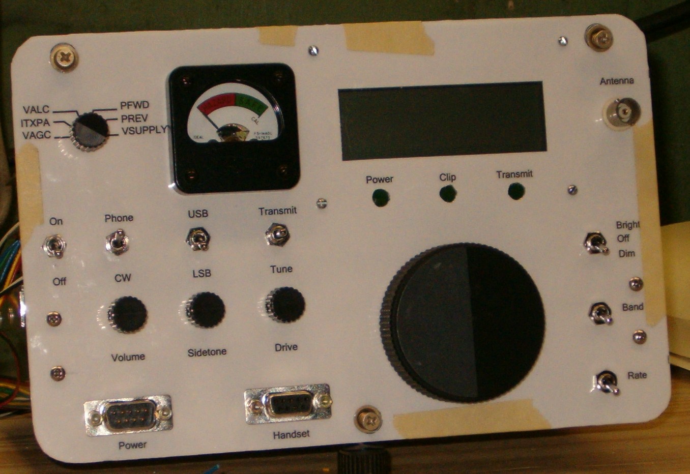
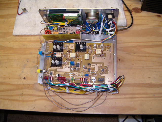
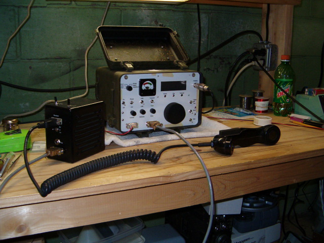
Here are some pictures of the radio:
Front panel close-up: Cropped_HPIM0121.JPG
Internals, top view: HPIM0138.JPG
Complete radio: HPIM0140.JPG
Anyway, here is a description of each of the boards.
Microcontroller
A PIC 16F877 microcontroller reads an optical encoder for operator frequency control input. The microcontroller decodes the pulses from the encoder and outputs a serial datastream to the DDS board and also drives a 20x4 Liquid Crystal Display (LCD) which indicates frequency of operation. At present, there are many unused IO pins that are available for future experimentation. The board also contains unused pads for various items like a serial EEPROM or Realtime Clock and power transistors. These extra pads were included for future experiments. Presently, I am running a very poorly hacked version of the SIGGEN3A code available from The New Jersey QRP Club (http://www.njqrp.org/ham-pic/siggen3a.asm.txt). I hope to post a copy of my version when it is in a presentable form and I have permission from its authors.
Schematic: Radio_control.pdf
PCB: Radio_ctrl_PCB.pdf
Synthesizer
The synthesizer consists of the famous Analog Devices AD9850 DDS chip followed by a pair of D-type flip flops which form a quadrature divider. The AD9850 generates a signal in the range of 0 – 41 MHz which is then divided in the quadrature divider to give four outputs in the range of 0 – 10.25 MHz. Each of the four divider outputs are separated in phase by 90 degrees. The four signals are buffered and passed through resistive voltage dividers before leaving the board. These signals form the I and Q local oscillator inputs of the receiver and exciter boards.
The AD9850 is presently responsible for limiting the upper frequency range of the transceiver. Since the highest frequency the AD9850 can produce is 41 MHz and we must divide that by 4 to get the quadrature signals, the highest local oscillator frequency we can get is 10.25 MHz. The AD9850 is also responsible for the less than desired receiver dynamic range due phase noise caused by its use of a 10 bit D/A converter. Don’t get me wrong; the AD9850 is still a great part, but we can do better. It is hoped that the synthesizer will eventually be upgraded to the AD9854 which will generate quadrature outputs on its own, without dividers, up to about 60 MHz. The AD9854 also has 12 bit D/A converters, which should result in better phase noise numbers. Stay tuned for developments.
Schematic: Synthesizer.pdf
PCB: DDS_PCB.pdf
Exciter
When the exciter is operating in the PHONE mode, microphone audio comes into the exciter board and goes to analog switch U17A (ADG436) where it is passed through to an external TX GAIN potentiometer. If CW mode is selected, a 750 Hz tone is generated by an RC phase shift oscillator, low pass filtered and passed to analog switch U17B where it is gated (keyed) in response to the signal from the KEY_IN signal. The keyed tone is then low passed filtered again and passed back to U17A. If the PHONE/CW signal is in the CW position, the keyed CW signal is passed to the TX_GAIN control; if the PHONE/CW signal is in the PHONE position, microphone audio is passed to the TX_GAIN control. The astute reader may notice that the RC oscillator has too much gain for producing a sinewave output. This will be fixed. The reader may also notice that provisions are made for supplying power to an amplified microphone; this can be removed by removing the jumper between R6A and C2. I mostly use amplified dynamic or electret microphones which require a DC power source and provide a high signal output. If other types of microphones are used, it may be desirable to increase the gain of the audio amplifier chain by increasing R28 or decreasing R27.
The audio from the TX_GAIN control is passed to U15 (OP413) where it is amplified. Q3 provides a means of reducing the audio drive in response to ALC voltage from the RF power amplifier board. At ALC = 0 volts, no gain reduction occurs. When ALC = 7 volts, the audio is nearly completely cutoff. This does provide a crude means of transmitter overdrive protection. Transmit audio is also low pass filtered to limit transmitted bandwidth. Another section of U15 amplifies the transmit audio to provide transmit sidetone, which is sent to the receiver board. The output from the low pass filter is fed to the phase shifter circuits and to U6, which detects when the TX_AUDIO level is too high. When TX_AUDIO exceeds 3 volts pk-pk, alternate sides of comparator U6 will fire, causing a front panel LED to illuminate. This provides the operator with an indication that the TX_GAIN control setting should be reduced.
A phasing exciter is more prone to causing adjacent channel interference due to audio distortion than a filter type transmitter. This is because the phase shift networks, to be discussed later, only provide the correct phase shift over a certain range of audio frequencies. Distortion in the audio chain produces harmonics which lie outside the normal voice range (300 – 3000 Hz). If harmonics are produced which lie beyond the range the phase shifters are designed for, cancellation of the undesired sideband will not occur. This will result in excessive bandwidth both in the direction of the intended sideband and in the direction of the undesired sideband. A filter type transmitter will pass only frequencies within the passband of the sideband filter, thus reducing the distortion products somewhat. Keeping the audio chain clean of harmonics is of the utmost importance in a phasing transmitter.
The next stop for the transmit audio is the audio phase shifters. Here the audio passes through two separate chains of circuits known as all-pass filters. These circuits pass all frequencies equally well but cause the signal to change phase as it passes through. The circuits are set up such that after passing through their respective shifter chains, two signals will be produced that will be equal in amplitude but differ in phase by 90 degrees. The phase shift circuit in the exciter was designed to provide a 90 degree phase differential over the range of 300 to 10,000 Hz. This was done because of the concerns for distortion, noted earlier. If the audio chain does produce distortion products above 3000 Hz, then at least those below 10,000 Hz will experience opposite sideband cancellation. Designing the phase shifter in this way results in somewhat lower performance for in band (300 – 3000 Hz) signals, but reduces the chance of causing serious out of band interference (splatter). Measured suppression of the undesired sideband was greater than 40 dB for in-band signals.
Traditionally, the audio phase shifters have been the most difficult part of a phasing radio circuit to obtain acceptable performance from. In the 1960s, the phasing method got a bad name because component tolerances and value drift over temperature made it difficult (or impossible) to maintain the required 90 degree phase difference through the phase shift circuit. Today, we can easily obtain resistors with 1% tolerances and capacitors with tolerances of 2%, making phase shifters of today much more practical than those of yesteryear.
The outputs of the phase shifters are applied to potentiometers R50 and R51, which are used to balance out and amplitude differences that might have occurred in the phase shifters. Their adjustment will be covered later. After amplitude balancing, the outputs of the phase shifters are applied to the inputs of an analog switch where sideband selection occurs. The two audio channels of audio are applied to buffer amplifiers in U11. The buffer amplifiers provide isolation of the relatively high output impedance of the shifters and the relatively low input impedance of the balanced modulators. Sideband selection occurs by selecting the upper buffer to the upper shifter and the lower buffer to the lower shifter when the sideband select signal is high and the reverse when the sideband select signal is low.
The two channels of buffered audio are separately sent to two Minicircuits SBL-1 balanced modulators (U13 and U15). The local oscillator signals, which are phase shifted 90 degrees to each other, are passed through Minicircuits MAR-8ASM MMIC amplifiers. These amplifiers raise the level of the local oscillator signals to about 0 dBm, as needed by the balanced modulators. The outputs of the balanced modulators are then summed in a resistive network and applied to U16, another MAR-8ASM MMIC amplifier where its signal level is raised to about 0 dBm.
Q100 provides another 10 dB of gain, raising the exciter output level to about 10 dBm.
A buffer consisting of Q1 and Q2 regenerates the Push To Talk (PTT) signal for transmit/receive selection. The RAW_PTT signal from the front panel connection is buffered and then distributed to other modules in the radio to ensure that all parts of the radio go between transmit and receive simultaneously. Without this buffer, it may be possible for an external PTT signal that did not pull all the way to ground to have some parts of the radio in an indeterminate state.
Schematic: Exciter_b1.pdf
PCB: Exciter_b_PCB.pdf
Receiver
The received signal passes through an external bandpass filter (discussed later) and comes to the receiver board where it is split and fed to two Analog Devices AD831 active mixers (U1 and U2). The mixers are also fed with I and Q local oscillator signals from the synthesizer board. The mixers each output audio signals that are identical to each other except that they are separated in phase by 90 degrees. The AD831 mixers were chosen because of their high signal handling capability and the fact that they exhibit conversion gain. Other mixers, such as the NE602 have gain but overload easily, while diode mixers handle lots of signal but exhibit several dB of loss.
The audio from these mixers are fed to an audio phase shift network consisting of U3 and U4 (Analog Devices OP413). The phase shifted audio is then fed to both a summing amplifier (upper U5), another OP413, and a difference amplifier (lower U5). Upper sideband audio will be available from the output of the summing amplifier, while lower sideband audio will be available at the output of the difference amplifier. The receiver phase shifters were designed to provide a 90 degree phase shift differential over a range of 300 to 5000 Hz.
An Analog Devices ADG436 analog switch is used to select the desired sideband from the sum or difference amplifier. The selected audio is then passed to an 8 pole low pass active filter with a cutoff frequency of about 3 KHz. This filter provides the main selectivity of the receiver.
The filtered audio is then passed to an AGC amplifier chain consisting of two, Analog Devices AD8367 Variable Gain Amplifiers (VGA), which provide approximately -6 to 90 dB of gain. The AD8367 contains an RMS responding output level detector which requires only a single capacitor to form the AGC feedback loop. The capacitor, C37, sets the AGC response time. An LM321 (U10) buffers the AGC signal for driving a front panel received signal strength meter.
The gain controlled audio is then made available to another analog switch (U11) where receiver audio or transmitter sidetone is selected, depending upon whether we are in transmit or receive mode.
The selected audio is then sent off-board to a front panel volume control potentiometer and then applied to an LM380 audio power amplifier. The amplified audio is then sent to an external speaker or handset.
The MDS of the receiver was measured at less than 0.1 uV. Undesired sideband suppression was measured at greater than 50 dB. Blocking dynamic range was measured at greater than 90 dB at 10 KHz separation.
Schematic: PhasingRX1.pdf
PCB: PhasingRX_PCB.pdf
RF Power Amplifier
The RF power amplifier is a three stage linear amplifier with the first two stages being single-ended and a push-pull configuration in the final output stage. A low value resistor (0.1 Ohm) in series with the DC supply to the final stage develops a voltage drop proportional to the DC current draw of that stage. The voltage developed across this resistor is amplified to drive a front panel meter for final amplifier current indication and is also used to develop ALC feedback voltage, which is fed to the exciter.
No schematic or PCB layout of the amplifier is presented at this time as I am still working on flattening the frequency response of this stage. More information will be presented when I am satisfied with the performance of this circuit.
Bandpass Filtering and Transmit/Receive Relay
In order to simplify the design of the transceiver and to achieve greater immunity from receiver overload, it was decided that bandswitching would be accomplished my means of plug-in filter modules. Several methods of bandswitching were investigated and each was rejected due to cost or performance issues. PIN diodes are often used in commercial radio designs to switch various band filters in and out of circuit, but this often leads to intermodulation distortion in the presence of strong RF fields. PIN diodes suitable for use at 1.8 MHz are also not readily available in small quantities to the experimenter. Relays could have been used but this would be rather bulky and expensive. A multipole rotary switch was also rejected due to extremely high cost and availability concerns.
In the final design, one board was used to contain two relays which perform the duties of switching the antenna between transmitter and receiver and also switch a bandpass filter between the receiver frontend and the exciter output. This board also contains two transistors which apply power to the relays when the RX/TX line is pulled low. A daughter board, upon which the actual filter components are mounted plugs into a PC board edge connector on the relay board. Filter boards are made up for the bands of interest and simply inserted when that band is desired.
The filter board contains a two resonator bandpass filter which serves as the receiver front end filter when in the receive mode and also filters the exciter output before applying it to the RF power amplifier input during transmit. A half wave (double Pi) circuit filters the output from the RF power amplifier. This filter is used during transmit only.
Schematic: BPF_SCH.pdf
PCB: BPF_board.pdf
Other Thoughts
While designing this transceiver, extensive use was made of computers. Considerable time was spent conducting Google searches into what technologies were available to use, how other people are doing things, and what kind of results they were getting. The internet contains a wealth of information for the radio designer; make the best of it!
Nearly every manufacturer of electronic components now has a website which features his products. These websites can be a goldmine of information. Not only from the obvious source of datasheets for a particular product, but for the many application notes that have been published over the years. Many of these are almost complete mini-courses in electronic design. Many manufacturers now also have (free) design tools on their websites which make designing a circuit much easier than ever before. Look for these tools and make use of them.
Some use was also made of computer simulations using an old version of MicroSIM. A circuit simulator lets you try things out before committing to a particular circuit. The phase shifters and audio filters were extensively simulated before the final design was chosen. The end result was a circuit that worked as expected the first time.
All of the schematics and PCB layouts as well as the mechanical design were all drawn using AutoCAD. Using a drafting program, such as AutoCAD, allows the designer to make many design changes and “tweak” the design until it is just the way you want it. It is much easier to move large chunks of circuit around on a computer screen that it is on paper. Using a drafting program allowed me to draw PC boards with the accuracy needed to handle chips with .025” pin spacings. The design of the front panel was also greatly aided by having the ability to place items on the panel and move them around until everything fit and had a neat appearance. A full blown package like AutoCAD is not needed; there are many low cost drawing packages available today that will serve the needs of the homebrewer very well.
Surface
This project made extensive use of surface mounted components. Since I make my own circuit boards, the decision to use surface mount components was an easy one. Using surface mount components eliminates the drilling of hundreds holes in the circuit board that would be required with through hole components. Surface mount components also tend to function more like “ideal” components than do their through hole counterparts due to their inherent lack of lead inductances.
Surface mount components are also much easier to work with than many people believe. Contrary to popular belief, an expensive set of tools is not needed. I use a pair of medical forceps to position the components on the pad and a Weller temperature controlled soldering iron with a 1/8” tip to solder almost everything. For some large power devices, I will use a 100 watt iron with a ½” chisel tip. Since my eyes are not so good anymore, I have two pairs of cheap reading glasses (+2 and +4 diopter) and a small handheld magnifier. The reading glasses allow me to focus on close-in objects while soldering and the magnifier allows inspection of the joint after soldering.
Fine pitched devices are soldered by positioning the part on the pads and tacking down the corner pins. A liberal amount of liquid flux is applied and a large blob of soldered is deposited across all of the pins. Solder wick is then used to remove excess solder. An inspection with the magnifier helps to reveal any voids or bridges. An Xacto knife helps to remove bridges. After soldering, wash the board in paint thinner to remove the flux and then a quick acetone bath to remove the paint thinner.
Rectangular components like resistors and capacitors can easily be soldered by applying a small blob to one pad on the board. While the solder is still liquid, place the component on the pad with the forceps and remove the soldering iron. When the solder is cooled, do the other end.
Homemade Printed
Circuit Boards
All of the modules in this project were built on circuit boards that were made at home. After the schematic is drawn, the board is laid out using AutoCAD. Using a drafting program allows accurate placement of the components and traces needed in the circuit. After the layout has been designed, it is printed on a special paper using a laser printer. The special paper, known as “Toner Transfer System” paper is available from Pulsar (http://www.pulsar.gs/), or from Digikey (www.digikey.com). After printing, the paper is applied to the circuit board using a heated press which melts the laser toner onto the bare circuit board. The paper is removed by soaking in water, leaving the toner adhered to the circuit board. The toner then acts as a resist when the board is etched. The board is etched in the normal manner using ferric chloride. Using this method, I can pretty consistently get traces down to .010” wide and .010” separations. After etching, remove the toner using acetone, followed by scrubbing with a mild abrasive cleanser such as Comet.
A few words of caution are in order about the Toner Transfer System. Pulsar claims it can be applied to the board using an ordinary clothes iron. My results using an iron were very disappointing. After spending $300 for their heated press, my results are now very good.
Techniks, Inc. (http://www.techniks.com/) also makes a system similar to that of Pulsar. You may want to check them out. Their system actually did work with an ordinary clothes iron but did not produce as sharp of traces as the Pulsar system. There is probably some technique involved in getting good results.
When I lay out my circuit boards, I use double sided board material but only put traces and components on one side. The other side is left unetched and forms a continuous groundplane. Whenever I need to make a connection from my circuit to ground, I simply drill a hole and run a piece of bus wire through it and solder on both sides. Having a groundplane available for the entire circuit generally makes for a stable circuit that does not normally require additional shielding.
Previously, I would solder coat the boards after etching. To do this, paint the board with liquid flux. Get a small glob of solder on the tip of your iron and quickly run it down the traces on your board. A bright coating of solder will stick to the trace. This makes later soldering of the components much easier.
The last couple of boards I have made have received silver plating, rather than solder coating. Pulsar sells their “Silverlining” kit which contains a powder that you rub onto the board with a damp rag. The exposed copper picks up a nice silver coating that takes solder very easily. Unlike solder coating, silver plating does not increase the width of your traces or cause accidental bridges between traces. A similar product is also sold by Cool-Amp (http://www.cool-amp.com/). A little bit of this stuff goes a long way, so, its not as expensive as it looks.
Panel Graphics
Until recently, whenever I was finishing up a project, I would paint the front panel and then use dry transfer lettering to label everything. After lettering, I would then spray with clear lacquer to protect the lettering. After it was all done, I would invariably notice an error in the lettering.
With this project, I tried a new method of lettering the front panel. I drew the panel graphics on the computer as I was laying out the panel. The graphics were then laser printed onto a piece of ordinary paper. A cutout was made in the paper for an LCD window, and then the paper was plastic laminated at a stationary store. This makes for a very neat layout. If an inkjet printer is used, you can use color in your graphics to enhance the appearance of your project.
Get going! Do Some Homebrewing!
While I really don’t expect anybody to really want to replicate this project, I hope it has given a few new ideas that may find use in your own projects. Happy homebrewing!
Contact
If you want to contact me, you can do so at:
[email protected] Replace “mycall” with wb9ipa
Useful Links
Design utilities
TI Design Utilities, FilterPro: http://focus.ti.com/analog/docs/articles.tsp?familyId=57&templateId=3&path=templatedata/cm/brc/data/20030307amplifierdesignutilities_home&articleType=brc
http://www.werewoolf.org.je/gj3rax.htm
Links to Vendors:
Digikey: www.digikey.com
Mouser Electronics: www.mouser.com
RF Parts, Inc.: www.rfparts.com
Links to Manufacturers:
Microchip: www.microchip.com
Analog Devices: www.analog.com
Minicircuits: www.minicircuits.com
National Semiconductors: http://www.national.com/
Linear Technology: http://www.linear-tech.com/
General Interest Articles:
Bandpass Filters: http://www.arrl.org/members-only/tis/info/pdf/001009qex013.pdf
Kk7b exciter article: http://www.arrl.org/tis/info/pdf/9304027.pdf
Kk7b receiver article: http://www.arrl.org/tis/info/pdf/t9301032.pdf
Philips Applications Note #1981: http://www.semiconductors.philips.com/acrobat/applicationnotes/AN1981.pdf
W9CF Analysis of audio phasing networks: http://fermi.la.asu.edu/w9cf/articles/phase/phase.html
Paper explaining Filter vs. Phasing Methods: http://www.northcountryradio.com/PDFs/column011.pdf
Mathematical explanation of SSB methods: http://members.tripod.com/michaelgellis/mixerscom.html
Good article on phase shift networks: http://home.att.net/~wa1sov/technical/allpass/allpass.html
Two landmark articles on phasing method. I have never been able to find copies of these articles to read, but, I would love to see them someday.
Norgaard, D.E., "The Phase Shift Method of SSB Signal Generation," Proc. IRE, (Single Sideband Issue), Vol. 44, Dec 1956. pp. 1718-1735
Norgaard, D.E., "The Phase Shift Method of SSB Signal Reception," Proc. IRE, (Single Sideband Issue), Vol. 44, Dec 1956, pp. 1735-1743
Very comprehensive list of references on phasing method: http://www.home.earthlink.net/~christrask/pshift.html
Additional sites of interest:
Markus Hansen, VE7CA, has done a wonderful job with his homebrew all band HF transceiver. Well worth taking a look at.
http://www.qsl.net/ve7ca/index.htm
Wes Hayward, W7ZOI, has lots of good homebrew information.
http://users.easystreet.com/w7zoi/