

|
|
Introduction
With today's state of the art, the operational amplifier package is well established as a means of obtaining voltage amplification and knowledge of how to design discrete transistor amplifiers for this purpose might seem unnecessary. Notwithstanding this, discrete transistor circuits are still needed at frequencies above the range of the operational amplifier and for certain special applications such as low noise amplification where a discrete transistor can often be made to perform better than the amplifier package.
In the paragraphs which follow, we will discuss factors which determine the gain of the transistor voltage amplifier and we will discuss an established method of determining the component values in the transistor circuit. The discussion will concentrate on the usual resistance capacity (RC) method of coupling and include such effects as loading by the following stage. The discussion essentially concerns the bipolar transistor but it will also extend to a problem in RC coupling the field effect transistor.
Current Transfer Ratio Hfe And Stage Gain
If you were to select a bipolar transistor for an amplifier to obtain maximum voltage gain, you might be tempted to select one with the highest current transfer ratio Hfe. In fact, this would be of no avail as voltage gain is essentially dependent on two factors, namely the emitter current (Ie) and the output load resistance (RL), but not Hfe. On the other hand, a high Hfe could increase the voltage gain of the previous stage. If these statements have astounded you, then just read on.
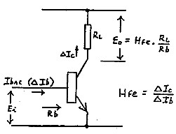 |
Figure 1 is a representation of the transistor operating as a voltage amplifier. The AC output voltage (Eo) is equal to the AC current at the collector multiplied by the load resistance (RL) and the AC current at the collector is equal to the AC current at the base (Ibac) multiplied by Hfe i.e:
Eo = Ibac. Hfe . RL....................... (1)
The AC current at the base is equal to the AC input voltage (Ei) divided by the transistor input resistance (Rb), i.e:
Ibac = Ei / Rb.............................(2)
Substituting (2) in (1) we get:
Eo = (Ei . Hfe . RL) / Rb
and voltage gain Av = Eo / Ei
= (Hfe . RL) / Rb.........................(3)
Based on expression (3), voltage gain is clearly dependent on Hfe but let us now examine Rb. According to theoretical text books, the input resistance (Re) of a common base connected transistor is derived as follows:
Re = (K.T)/(Q.Ie)
where K = Boltzmann's Constant
T = Absolute Temperature
Q = Charge of an Electron
Ie = Emitter Current in mA
At room temperature this works out to Re equal to about 25/Ie. For common emitter connection, input is to the base and input resistance is Rb. Base current equals collector current (Ic) divided by Hfe. Emitter current (Ie) = Ic + Ib. However Ib is small compared to Ic and for the purposes of this exercise, we can consider Ie and Ic to be near equal. Hence, with near constant voltage across the base/emitter forward biased junction, input resistance (Rb) is multiplied by Hfe. Thus we get:
Rb = (25.Hfe) / Ie........................... (4)
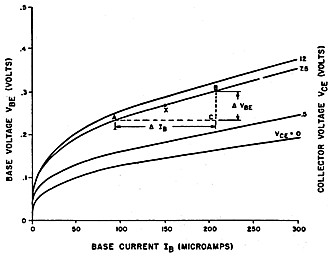 |
To illustrate the variation of AC base resistance with variation in base current (Ib = Ie / Hfe), figure 2 is shown. Observe how the slope of the curves (and hence the value of Rb) decreases as the base current is increased. Rb is given by the ratio of change of voltage base/emitter (Vbe) to change in base current (Ib) i.e. Δ Ebe / Δ Ib.
If we now substitute expression (4) for Rb in expression (3), we get a further expression for voltage gain:
Voltage gain Av = (Hfe . RL . Ie) / (25 . Hfe)
Hfe is cancelled out so that:
Voltage Gain Av = (RL . Ie) / 25............... (5)
Observe that calculation of voltage gain now only involves the values of RL and Ie and not Hfe, so that our first point has been proved.
In Summary, the signal voltage at the transistor stage output is proportional to the input signal current fed into the transistor base multiplied by the output load resistance (RL) and the current transfer ratio (Hfe). The input signal current is equal to the signal voltage at the input divided by the AC base resistance. This base resistance (Rb) is an inverse function of the current running in the emitter but it is also proportional to the current transfer ratio. In evaluating the ratio of output signal voltage to input signal voltage (i.e voltage gain Av) from these factors, we find that the current transfer ratio can be eliminated from the final formula and calculated voltage gain is essentially independent of the value of the current transfer ratio.
The Previous Stage
 |
As a further exercise, let us examine the amplifier stage shown as V2 in figure 3. Referring to previous paragraphs, we have seen that its voltage gain is independent of Hfe but we have also seen in expression (4) that Rb is directly related to Hfe and a low Hfe means a low value of Rb.
We now examine the gain of the previous stage V1. The collector load resistance of this stage is the parallel result of collector resistor RL1, the V2 stage base bias resistors R1 - R2 and the input resistance Rb of V2. Rb is normally the lowest value making it the main factor in setting the load resistance of V1. Referring back to expression (5), we see that, for a given value of Ie in V1, the voltage gain of V l is controlled by its load resistance which is essentially the value of Rb in V2. A high value of Hfe in V2 gives a high value of Rb in V2 and this is reflected as high gain in V1. This confirms the second point which was made earlier.
Circuit Design
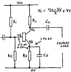
Design of a transistor voltage amplifier stage, as shown in figure 4, is really quite simple. Resistors R1 and R2 form a voltage divider which sets the base reference voltage. Resistor Re provides DC feedback to stabilise the emitter current and hence the operating point of the transistor. Resistor RL is the collector load resistor.
 |
The first thing is to decide on what emitter current should be used. A current of around 1 mA is usually quite satisfactory for audio amplification unless there is some special reason for selecting otherwise. If a low noise level stage is required, such as that following a low level high impedance microphone, a lower current might be desirable. On this subject, the reader is referred to an article by the writer entitled "Amplifier Noise" published in Amateur Radio, November 1985. On the other hand, a higher current is often required at higher frequencies and this will be discussed later.
The next decision is to select an emitter voltage (Ve). The higher this voltage, the greater is the emitter current stability in the presence of temperature variation and for variation in the value of Hfe. A value of Ve around 1 to 2 volts is normally satisfactory. If the supply voltage Vcc is around 12 volts, one might select Ve = 2V. For Vcc = 6V, a value of Ve = 1V might be as high as one can go. Calculate resistor Re as follows:
Re = Ve / Ie
Now work out the voltage at the base. For a germanium transistor, this is close to 0.2 V higher than that at the emitter. For a silicon transistor, this is close to 0.7 volt higher than that at the emitter. Of course, this differential is simply the forward voltage drop across the base to emitter diode junction.
The base current is equal to the collector current (or emitter current) divided by Hfe. (Note that collector current is nearly equal to emitter current.) The idea is then to bleed a current through the R1-R2 divider about 10 times the base current so that the base voltage is held constant, almost independent of the base current. We calculate the resistance values as follows:
R1 = (Vcc - Vb) / 10 . Ib)
= Hfe . (Vcc - Vb) / 10 . Ie)
R2 = Vb / (9 . Ib)
= (Hfe . Vb) / (9 . Ie)
The reason why R2 calculation is divided by 9.Ib and not 10.Ib is that one tenth of the current is passed into the base itself.
All we have to do now is to work out a value for RL so that the operating point is set correctly. As far as the signal is concerned, the available supply voltage is (Vcc - Ve) and to make use of equal voltage swing either side of the operating point, the collector voltage Vc is set half way between Vcc and Ve. For RL, we calculate as follows:
RL = (Vcc - Ve) / (2 . Ie)
Operation is illustrated in figure 5 by the load line A for RL. Observe that the operating point is set at half the available supply volts.
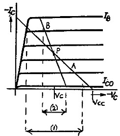 |
Figure 5. Load lines for amplifier stage. A = Load line for collector resistor (RL) only {Maximum signal voltage swing (1) approaches half supply voltage}. B = Load line with coupled load {Maximum signal voltage swing (2) is reduced}. |
Effect Of Coupled Load
As discussed previously, one effect of a coupled load, such as a following transistor, is to lower the effective load resistance and lower the gain of the stage. Another effect is to lower the maximum signal voltage swing which can be achieved. This is demonstrated in figure 5 by load line B for the total parallel load.
One way to increase the maximum signal voltage swing is to lower the value of RL. This of course means a circuit design around a higher value of collector current.
Another way to increase the maximum signal voltage swing is to reduce the signal loading by coupling via an emitter follower stage as shown in figure 6. The follower is characterised by high input resistance which reduces the signal loading. It also provides a low resistance signal source to drive an output circuit or another stage.
 |
The Field Effect Transistor And RC Coupling
From our previous discussion, the operational collector voltage is correctly set by selecting the collector load resistance RL for a voltage loss equal to half the available supply voltage. In the circuit of figure 4, the collector current is precisely set by the values of R1, R2 and Re and virtually unaffected by any spread in the bipolar transistor characteristics. With the field effect transistor (FET), the use of RC coupling can present quite a problem when a load resistance is placed in the drain circuit. Drain current is set by the bias voltage applied to the gate of the FET and unfortunately the drain current versus gate voltage characteristic of the FET varies from sample to sample of the same transistor type. If a resistance loaded drain is used, gate bias must be set to suit the individual transistor.
At radio frequencies, the drain resistor can be avoided by coupling via an RF choke, transformer primary or tuned circuit in series with the drain.
The Capacitors
To complete our discussion on the design of the basic circuit (figure 4) we still have to select the capacitors. Resistor Re is used to provide DC feedback for stabilisation of the operating point but this must be by-passed by capacitor Ce to prevent negative feedback at signal frequency. A good rule is to select the value of Ce such that its reactance is not greater than one tenth of the value of Re at the lowest frequency of operation.
Capacitor Cc provides DC isolation between the collector circuit and the following load circuit or following stage. Its capacitance value is selected such that its reactance is not greater than the reflected load resistance (perhaps the base resistance of the following stage), at the lowest frequency of operation. If equal to that resistance, it will give 3 dB loss at that frequency to form the low frequency pole.
High Frequency Operation
It was stated earlier that a collector (and emitter) current of around 1 mA was generally suitable for audio frequency voltage amplifiers. At higher frequencies, collector current has to be increased. The reason for this is that the value of load resistance RL must be lowered to make it low relative to the shunt capacitive reactance, inherent at the transistor output and at the following stage input. As frequency is increased, the shunt reactance becomes lower and hence RL must also be made lower. To maintain collector voltage at half the available supply voltage, collector current must be increased with proportional decrease in the values of R1. R2 and Re. Referring back to expression (5), gain is lost by the lower value of RL but this is compensated by the increase in Ie.
In the previous paragraph, we have been specifically discussing RC coupled stages with an implication of wideband operation. At radio frequencies, we might choose to tune the amplifier and incorporate the shunt capacitance as part of the tuned circuit so that a high load impedance is formed to provide higher gain. As our subject is essentially about RC coupled stages, we will not dwell further on that particular application.
The Emitter Follower
The emitter follower is a very useful special form of voltage amplifier. It has high input resistance, low output resistance and a gain just less than one. Its input resistance is approximately equal to the load resistance at its output circuit multiplied by Hfe. If base stabilising resistors are used as shown by R1 and R2 in figure 7, these must also be considered as part of the input resistance in parallel and in fact when used, are usually the main input resistance determining factor.
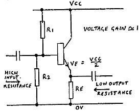 |
Output source resistance is approximately equal to the resistance of the source driving the follower stage divided by Hfe. In calculating the output source resistance, resistors R1 and R2 must also be taken into account as being in parallel with the input source. If the follower stage is RC coupled from a previous collector circuit, the collector load resistor can be taken to be the source resistance as the inherent output resistance of a common emitter stage is very high by comparison to the value of that resistor.
Calculation of R1 and R2 is the same as described previously for the common emitter amplifier except that base voltage Vb is made equal to half the supply voltage (Vcc) plus the base to emitter diode voltage (0.2V for germanium and 0.7V for silicon). Emitter voltage is then equal to half Vcc to enable equal signal voltage swing either side of the operating point and
Re = Vcc / 2 . Ie.
The problem of the coupled load limiting the signal voltage swing still applies to the emitter follower stage and the choice of emitter current (Ie) depends on just what value of coupled load resistance must be driven and how much signal voltage is required across that resistance. For low resistance coupled loads, quite a high emitter current is often required with low values of Re, R1 and R2 and consequently a high power dissipation transistor.
Defining A Fixed Stage Gain
Negative feedback can be used on any amplifier to achieve a defined stage gain. Providing the gain with feedback is a low value compared with that without feedback, the gain is set purely by the components which determine the proportion of feedback. This principle is well established in the application of operational amplifiers. In the case of the single transistor stage, the feedback can be achieved by removing the emitter bypass capacitor or dividing the emitter resistor into two separate components, only one of which is bypassed as shown in figure 8.
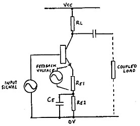 |
Providing the resultant gain is small compared to that without feedback, voltage gain is equal to the ratio (Re1 + RLt) / Re1. The value RLt is the effective load and the parallel result of RL, and the coupled reflected load. To determine the values of Re1 and Re2, calculate as follows:
Re1 = RLt / (Af - 1)
where Af is the desired gain
Re2 = Re - Re1
where Re is the value calculated to set the emitter current to the desired figure.
Stable voltage gains, defined by Re and RLt are achievable up to a value of around 10. Above that, transistor gain within the amplifier loop is insufficient to maintain dependence only on the feedback factor and the gain with feedback is then also a function of the amplifier gain without feedback. i.e.
Af = Av/(1 + βAv)
Where Av = gain without feedback
and β = the feedback factor or proportion of feedback.
Voltage & Power Amplification
The definitions of voltage amplification and power amplification go back to the days of valve amplifiers. The basis of these definitions is that in class A operation the valve does not consume power at its control grid and the requirement is to supply signal voltage rather than signal power to its grid. The last stage is a power amplifier because it must supply power to the loudspeaker or other load. All the previous driver stages are voltage amplifiers, their function being to raise the signal level sufficiently to drive the power amplifier. Field effect transistor amplifiers, with their high input resistance, can be considered in the same light but the writer could well be taken to task in defining the bipolar transistor stage as voltage amplifier when it is required to drive another bipolar transistor stage. The transistor is driven by signal current and hence the following stage consumes power. If one must be pedantic, the previous stage could well be considered as a power amplifier. Notwithstanding this, the circuit analysis discussed has been carried out on the basis of stage voltage gain and as such, the coupled stages have been considered as voltage amplifiers. This analysis concept then makes it compatible with analysis for the FET amplifier, the valve amplifier and operational amplifier circuitry.
Summary
A short discussion has been presented on the transistor voltage amplifier with particular reference to resistance capacity coupling. Included in the discussion is, the calculation of stage gain and a method of deriving component values in the amplifier circuit. Also included are the effects of a coupled load on gain and maximum signal voltage swing and an introduction to the emitter follower and stabilised gain amplifiers.
Addendum (Not in original article) - A Short Cut
To save going through the formulae, for the general case you might like to take a short cut to determine resistance values for the RC bipolar stage using a silicon transistor.
Select the emitter current as 1 ma.
Set the emitter resistor to 1500 ohms.
Set the collector resistor to half (Vcc - 1.5) x 1000 ohms
Assume hfe to be around 100 and:
Set base resistor R1 = (Vcc - 2.2) x 10,000 ohms
Set base resistor R2 to 24,000 ohms
This should provide an emitter voltage of 1.5V and a collector voltage set half way between Vcc and the emitter voltage to achieve equal positive and negative signal swing.
Symbols used in Text
Ei = Signal Input Voltage
Eo = Signal Output Voltage
Hfe = Forward small signal transfer ratio (or α)
RL = load resistance at collector
RL = Collector Resistor (equal to RL for stage unloaded)
Rb = Base Input Resistance
Re = Emitter Input Resistance
Ic = Collector Current in mA
Ie = Emitter Current in mA
Ib = Base Current in mA
Ibac = AC Signal Current at base
Av= Stage gain without feedback
Af = Stage Gain with feedback
β = Feedback factor