
IC18  VCO#5 T20
IC1   VCO#4 T1
IC4   VCO#3 T2
IC9   VCO#2 T9
The above are all located on the PLL board.
The VCO for IC17 is actualy one out of four different VCO's selected on the RF board. Which one of these depends on what band is selected.
   diode        controls                in              out (cut)
   -----        --------                ----------      ----------
   D65          mode confirmation       Morse           single beep
   D66          display resolution      100 Hz          10 Hz
   D67          memory protect          none            on
   D73          CW shift                800 Hz          400 Hz
   D78          WARC 24MHx band tx      disabled        enabled
   D79          WARC 18MHz band tx      disabled        enabled
   D80          General Coverage tx     disabled        enabled
Self-Test: You can run a rather complete test of the control logic by the built-in "semi-self-test", a series of 56 routines. To run this, turn the unit on whilst holding the AM and T-F SET switches pushed in. It changes to the next test when you turn the VFO knob clockwise. Turn the power OFF to reset the unit.
   Test         What it does
   ----         ---------------------------------------------------
     0          all positions in display light
     1          all segments in display dark
     2          all positions in display light
     3          all segments in display dark
     4          one digit lighted (rightmost)
     5          next digit lighted
     6          next digit lighted
     7          next digit lighted
     8          next digit lighted
     9          next digit lighted
    10          next digit lighted
    11          next digit lighted
    12          next digit lighted
    13          next digit lighted
    14          next digit lighted
    15          next digit lighted
    16          next digit lighted (leftmost)
    17          beeper sounds
    18          beeper silent
    19          all mode LEDs ON
    20          all mode LEDs OFF
    21          receive
    22          transmit
--------------------------------------------------------------------------
The following tests change internal signals. They are most useful if you
are trying to trace the circuits controlled by these signals.
    23          Band select - all lines high
    24          BAND select - all lines low
    25          PD select - all lines high
    26          PD select - all lines low
    27          ENF select - all lines high
    28          ENF select - all lines low
    29          ENP select - a:ll lines high
    30          ENP select - all lines low
    31          RES select - all lines high
    32          RES select - all lines low
    33          CO select - all lines high
    34          CO select - all lines low
    35          AX select - all lines high
    36          AX select - all lines low
these next tests check the outputs of the 8255 parallel port interfaces,
which select several internal functions.
    37          (IC2) port A all lines high
    38          (IC2) port A all lines low
    39          (IC2) port B all lines high
    40          (IC2) port B all lines low
    41          (IC2) port C0-C3 high, C4-C7 low
    42          (IC2) port C0-C3 low, C4-C7 high
    43          (IC53) port C all lines high
    44          (IC53) port C all lines low
Following display busy lines and scan lines in the rightmost 9 digits of
the display. You will push buttons to cause the digit to change from a 1 to a 0
indicating that the associated button has been pushed.test bit8 bit7 bit6 bit5 bit4 bit3 bit2 bit1 bit0 ---- ---- ---- ---- ---- ---- ---- ---- ---- ---- 45 LOCK AT Mic UP Mic DN PTT/AT VS1 46 (none) 47 (key scanner) 48 1 6 V/M VOICE 49 2 7 M>V RIT A/B 50 3 8 SCAN XIT SPLIT 51 4 9 M.IN T-Fset A=B dip3 dip4 dip5 52 5 0 CLEAR 1Mhz dip1 dip2 dip6 dip7 53 ENT DOWN UP dip8 dip9 dip10(the digits 0-9 are on the front panel keyboard; dip2-dip10 are the segments of S50, the SSB frequency response dipswitch on the rear of the control unit printed circuit board.)
                ACC-1 Serial Interface
        pin     signal
        ---     ----------------------------------------------------
         1      signal ground
         2      data from transceiver
         3      data to tranceiver
         4      cts to transceiver - computer can throttle output
         5      cts to computer - transceiver can throttle input
         6      no connection
SSB frequency response dipswitch: located on the back of the control unit,
this adjusts the frequency response of the upper and lower sideband modulators
to compensate for component variations. Changing it isn't a good idea, since you
have to have a two-tone oscillator and have to reset the carrier suppression
adjustment if you do. The service manual explains this process; I'm including
this here so that people who have been wondering what the dipswitch does won't
screw themselves by flipping switches to see what happens. tweaker what it does
------- -----------------------------------------------
RF-VR3 FM Microphone Gain
RF-VR6 FM Deviation - set to 4.6KHz on dev meter
IF-VR2 S-meter zero - set to zero with 50 ohm dummy load
IF-VR3 S-meter S9 - set to S9 with 40dbu input 14.175MHz USB
IF-VR4 Squelch threshold - close at 12 o'clock with
mode = CW and filter WIDE
IF-VR9 CW side tone level - as you like it
IF-VR10 Beep tone level - as you like it
Someone wanted to know what the difference between the DATA connections on
ACC-2 and the AFSK connectors was. On output, none; the AFSK and the DATA out
pin on ACC-2 are connected together, and are fed from the high side of the
volume control - they are receiver audio BEFORE the cw sidetone, beeper, and
voice response unit are mixed in, and should be a constant level independent of
the AF gain setting. The AFSK input is different from the DATA IN connection;
AFSK and microphone signals both go through the mike preamp and speech
processor; the DATA input bypasses both. The MIC GAIN pot does control all three
input levels.
                   ____ 4    3    2    1
       GROUND ___ |
                  |____ 8    7    6    5
                  |
                  |___ 12   11   10    9____________
                           /                        |
       MIC    ____________/    13                   |
                                |                   |
                                |                   |
                               \_/                 \_/
                              =====               =====
                                |                   |
                                |___________________|
                                           |
                                           |
                                           |
                                           |

                                          PTT

       Pins        |           Application
     -----------------------------------------------------------------

        3              Data output - not used as the level is very low
                       the prefered connection is via the speaker output
                       this also allows fine adjustment of level to
                       enable best decoding. (A switch on the speaker to
                       'mute' it when required is a good idea.)

        4              Ground - you may have to experiment with these
        8              connections to eliminate RF feedback and noise.
       12              Here they are all strapped.


        9              Mic mute - prevents audio pickup from the mic when
                       earthed. By connecting to the PTT line as shown
                       through a diode automatically MUTES the mic when
                       using data. When the front panel PTT or MIC PTT
                       are used the microphone is 'live'.

      13               Standby - PTT which when taken to ground puts the set
                       'on air'. By connecting through a diode as shown
                       doesn't affect the PTT operation but allows auto
                       mic muting.
The diodes used can be virtually anything, here they are
IN4148. IC 54 is a uPD-8251-AC Serial Communications Interface.
Commonly called an 8251A ($1.89 Mail Order)
IC 55 is a TC-4040-BP 12 Stage CMOS Divider.
Commonly called a 4040 ($0.69 Mail Order)
The IC-10 Interface Kit from Kenwood Contains ONLY these two parts and
less instructions than are in this file. The only thing you are going to miss,
is the $22+ price tag on the IC-10 Kit.Signals are TTL levels (NOT RS-232) Baud rate is 4800 (1200 Opt.) Format is ASCII Serial; 1 Start, 8 Data, 2 StopsThe Baud rate may be changed to 1200 Baud by removing jumper W50 and installing a jumper from the left pad to the center pad as viewed from the front of the radio. This will become obvious once you have the radio opened up. Many other Baud rates are possible, just look at the schematic.
ACC-1  Connector                  Use a 6 Pin DIN Connector.
                                         (Radio Shack $1.29)
Pin     Signal  Comments
________________________

1       Gnd     Signal Ground
2       TXD     Serial Data from Radio to Computer
3       RXD     Serial Data from Computer to Radio
4       CTS     Computer Ready;  (Radio Input)
5       RTS     Radio Ready;    (Radio Output)
6               No Connection

Pins 4 and 5 may be left Unconnected.


***** Command Description for Kenwood Computer Interface *****
______________________________________________________________

                Auto Information
                ________________
AIn;
                The Radio Will Send the Status Info Automatically
                Whenever the Operator Manually Varies any Function
                on the Radio which is Covered in the IF; Command
                        Where   n = 0 for Auto Info OFF
                                    1 for Auto Info On

                The Status Information Will be Sent in the Form :
                        As defined in the IF; Command


                Display Memory
                ______________
DMnnnn;
                This is a Factory Diagnostic Function
                and is of no practical use to the operator

                The Contents of the MPU Memory will be Read
                        Where   nnnn = MPU Address (0000 Thru FFFF (HEX))

                The Contents of the MPU Memory Will be Sent in the Form :
                 DMnnnn-aabbccddeeffgghhiijjkk;
                        Where   nnnn = MPU Address (0000 Thru FFFF (HEX))
                              aa~~kk = Hex Number Pairs Of Next 16 Locations


                Down
                ____
DN;
                The Frequency or Memory Channel
                Will Decrement One Step


                Frequency VFO A / VFO B Request
                _______________________________
FA;
FB;
                The Frequency in the Selected VFO Will be Read

                The Frequency Will be Sent in the Form:
                 FAggmmmkkkhhh;   or
                 FBggmmmkkkhhh;
                        Where    gg = GHz. Value
                                mmm = MHz. Value
                                kkk = kHz. Value
                                hhh =  Hz. Value


                Frequency VFO A / VFO B Select
                ______________________________
FAggmmmkkkhhh;
FBggmmmkkkhhh;
                The VFO Selected Will be Set to the Frequency Defined
                        Where    gg = GHz. Value (May be sent As 00 or Spaces)
                                mmm = MHz. Value
                                kkk = kHz. Value
                                hhh =  Hz. Value


                Function Select
                _______________
FNn;
                The Function Defined Will be Selected
                        Where   n = 0 for VFO A
                                    1 for VFO B
                                    2 for MEMORY

                Identify Model Request
                ______________________
ID;
                The Model of the Radio Will be sent in the Form :
                 ID00n;
                        Where : n = 1 for a TS-940 (*)
                                n = 2 for a TS-811 (*)
                                n = 3 for a TS-711 (*)
                                n = 4 for a TS-440


                Read Information Request
                ________________________
IF;
                The Status Information Will be Sent in the Form :
                 IFggmmmkkkhhh     snnnzrx yytdfcp
                        Where   gg~~hhh = Value as defined in FA Command
                                      s = "+" or "-" Value of RIT/XIT
                                    nnn = Value of RIT/XIT (n.nn kHz.)
                                      z = "0"  (Not Used in TS-440)
                                      r = Value as defined in RT Command
                                      x = Value as defined in XT Command
                                     yy = Memory Channel No.
                                      t = 0 for Receive
                                          1 for Transmit
                                      d = Value as defined in MD Command
                                      f = Value as defined in FN Command
                                      c = Value as defined in SC Command
                                      p = Value as defined in SP Command


                Lock Knob
                _________
LKn;
                The Manual Frequency Control Functions Will be Disabled
                        Where   n = 0 for Lock OFF
                                    1 for Lock ON


                Memory Channel Select
                _____________________
MCxmm;
                The Memory Channel Defined Will be Selected
                        Where:  x = Don't Care   (Use "0" or Space)
                               mm = Memory Channel No. (00 thru 99)


                Mode Select
                ___________
MDn;
                The Mode Defined Will Be Selected
                        Where:  n = 1 for LSB
                                    2 for USB
                                    3 for CW
                                    4 for FM
                                    5 for AM
                                    6 for FSK


                Memory Read
                ____________
MRnxrr;
                The Memory Channel Defined Will be Read
                        Where:  n = 0 for RX VFO
                                    1 FOR TX VFO (Split Channels Only)
                                x = Don't Care      (Use "0" or Space)
                               rr = Memory Channel No.    (00 thru 99)

                The Memory Information will be sent in the Form :
                 MRn rrggmmmkkkhhhdz    ;
                        Where:  n = 0 for RX VFO
                                    1 FOR TX VFO (Split Channels Only)
                               rr = Memory Channel No.    (00 thru 99)
                         gg~~hhh = Value as defined in FA Command
                                d = Value as defined in MD Command
                                z = "0"  (Not Used in TS-440)
                        (Note: Four trailing Spaces)


                Memory Write
                ____________
                 MWnxrrggmmmkkkhhhdzxxxx;
                The Memory Selected Will be Set to the Frequency Defined
                        Where:  n = 0 for RX VFO
                                    1 for TX VFO (Split Channels Only)
                                x = Don't Care  (Use "0" or Space)
                               rr = Memory Channel No.    (00 thru 99)
                          gg~~hhh = Value as defined in FA Command
                                d = Value as defined in MD Command
                                z = "0" (Not Used in TS-440)


                RIT/XIT Clear
                _____________
RC;
                The RIT/XIT will be set to 0.00 kHz.


                RIT/XIT Down
                ____________
RD;
                The RIT/XIT will Decrement by 0.01 KHz. (10 Hz.)


                RIT/XIT UP
                __________
RU;
                The RIT/XIT will Increment by 0.01 KHz. (10 Hz.)
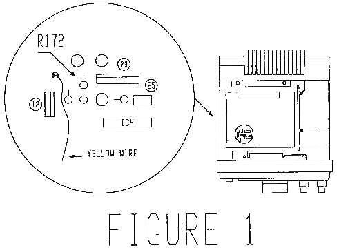
With some TS-440S transceivers, insufficient modulation may occur when the MC-85 compression switch is turned on. This may be caused by too much of a voltage drop across resistor R172 on the IF unit of the transceiver . If this is found to be the case, change the resistor from 1K ohm to 100 ohms.
Required part
100 Ohm, 1/6 Watt resistor (RD14CB2C101J)
PROCEDURE:
This modification may be covered under warranty.
Time required for this
modification is 0.5 hrs or less.
19-07-1998 TS-440S Notch filter low frequency
improvements
Author:
Trio-Kenwood Communication, inc.
The low frequency attenuation characteristics of the notch filter can be improved by reducing the input level to the notch filter chip (IC1). To compensate for the loss of input level, the amount of negative feedback to the audio amplifier (IC7) will need to be reduced. This modification is already incorporated in all models beginning with serial number 704XXXX.
Required parts:
120K Ohm, 1/6 Watt resistor ........ RD14CB2C124J
390 Ohm,  1/6 Watt resistor ........ RD14CB2C391J
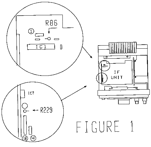
This is an optional change that may not be performed under warranty.
Time
required for this modification is 0.5 hrs or less.
19-07-1998 TS-440S Protecting
Q33
Author: Trio-Kenwood
Communication, inc.
If pin 7 (RL) of the remote connector is accidently connected to ground, current from the 14 volt line (14L) will damage transistor Q33 on the IF unit. This will prevent the radio from transmitting. To protect Q33, a 4.7 ohm resistor should be installed in series with the RL line on the foil side of the IF board. In the event that pin 7 is connected to ground, the resistor will open, but the transceiver will still be capable of transmitting.
Required part:
4.7 Ohm, 1/6 Watt resistor ........ RD14CB2C4R7J
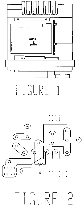
This is an optional change that may not be covered under warranty.
Time
required for this modification is 0.5 hrs or less.
19-07-1998 TS-440S Case Screws binding in the
heat sink
Author: Trio-Kenwood
Communication, inc.
Occassionally a case screw that fastens to the heat sink of the TS-440S will cross thread or bind when it is being inserted or removed. Binding may be caused by tooling marks on the screw or by burrs on the tapped threads in the heat sink. When a screw starts to bind, DO NOT TRY TO FORCE IT! as this may cause the head to shear off. If the screw is being removed and it starts to bind, return the transceiver to KENWOOD. Do not make attempts to remove the screw. In addition, if a transceiver is being brought to you with a scrw sheared off, return the unit to KENWOOD. Do not attempt to drill out the screw.
If a screw starts to bind when it is being installed, carefully back it out.
Inspect the screw for marks or burrs and replace it if it is questionable. Since
the threads in the heat sink may be causing the screw to bind, they should be
cleaned by running a 3 x 0.5 mm tap into each hole.
The tap is inexpensive
and can be obtained at may of the larger hardware stores.
To avoid cross threading, make sure the covers are properly aligned when they
are being installed. Proper alignment means that there is a clear path for the
screw to turn into the heat sink.
This assures that the screw does not rub
against the case and result in it turning into the heat sink at an
angle.
19-07-1998 TS-440 RX
Audio Mods
Here's some easy modifications to improve the rx audio
fidelity of Kenwood TS-440's. All references below are to the IF board component
designations.
When intermittent problems such as erratic display, loss of front panel control, or frequency lock-up are encountered, the PLL and Control circuits must be checked to determine which circuit is malfunctioning. While any number of components may cause such problems, if the Control circuit is suspect, there is a possibility that the ROM socket is at fault. The socket should be tested to determine if it is making good electrical contact with each pin on the ROM. If it is found to be defective, remove the socket and solder the ROM directly to the board. The ROM is IC52 on Control unit (B/2). It should be noted that units with serial number of 909xxxx and above do not incorporate a socket.
Caution
Removing the socket requires good soldering skills. The ROM is mounted on the Digital A unit and is designated as IC2. The board, being double sided, has solder connections on both component and foil sides. When the socket is removed, it is very important to insure that each pin is completely solder free. Having to pry up on the socket means that it is not completely desoldered and will cause the circuit foils to tear.
When performing any work on the Control boards, CMOS handling techniques must be observed. Such techniques include using a grounded or isolated soldering tip, avoid touching the pins of IC chips with your fingers, and ground yourself with a wrist ground strap.
To remove the socket:
This modification may be covered under warranty during the warranty
period.
Time required for this modification is 1.5 hour or
less.
21-04-2000 TS-440S
PLL unlock due to VCO #5
Author:
Kenwood Communication, inc.
The VCO and active low pass filter are sealed in synthetic rubber to mechanically stabilize them during mobile operation. Over a period of several years, the rubber's insulation properties can break down. This may be caused be repeated temperature variations. This can cause the VCO to vary in frequency which will force the loop to unlock or cause the audio to warble.
This modification will correct or prevent an unlock caused be VCO #5.
Required parts:
2SC2459(BL)      Transistor          QTY. 2
1SV153           Varactor diode      QTY. 1
Time required to perform this modification is 1 hour or less.
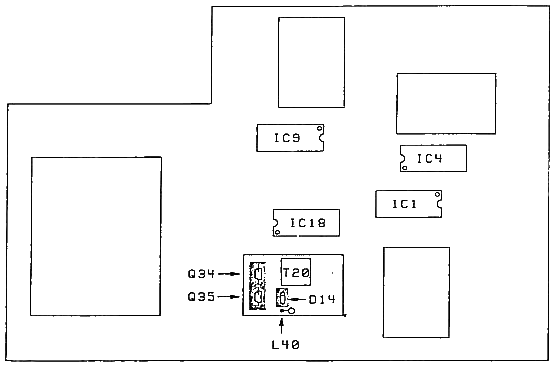
21-04-2000 TS-440S PLL unlock due to VCO
#1
Author: Kenwood
Communication, inc.
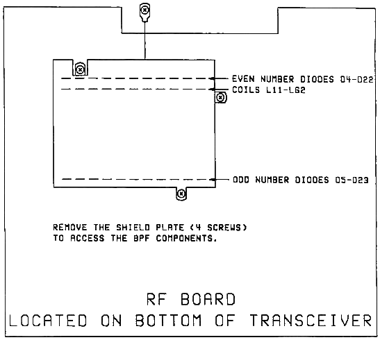
The TS-440S Control unit supplies band information to four circuits in the transceiver. The circuits are the receiver front end Band Pass Filter (BPF), the antenna tuner (AT), the transmitter Low Pass Filter (LPF), and the VCO circuits on the RF board that are part of PLL #1.
There are ten receiver front end BPFs that are diode switched into operation. If one of the diodes (D4-D23) becomes shorted or leaky, the band information is felt at two BPFs at one time. The voltage going through the bad diode will loop back to the VCO circuit, antenna tuner circuit, and LPF circuit.
The unwanted voltage will then create one or more of the following symptoms:
The most common symptom is the PLL unlock. To test the diodes, remove the large shield on the RF board to expose the BPF circuits. Reset the transceiver by holding in the A=B button as power is turned on. Even if the display only shows decimals, only the BPF for 14 MHz should be turned on. Using a DC voltmeter, measure the voltage at coils L11, L15, L21, L28, L34, L40, L46, L52, L58, and L62. Only coil L52 should measure 8 Vdc. The other coils should read 0 Vdc. If one reads 0.5 - 8 Vdc, replace the two diodes in that BPF circuit.
Coil/Diode/frequency range relationship:

L11  D4   D5           0 - 0.5 MHz        L15  D6   D7         0.5 - 1.6 MHz
L21  D8   D9         1.6 - 2.5 MHz        L28  D10  D11        2.5 - 4 MHz
L34  D12  D13          4 - 6 MHz          L40  D14  D15          6 - 7.5 MHz
L46  D16  D17        7.5 - 10.5 MHz       L52  D18  D19       10.5 - 14.5 MHz
L58  D20  D21       14.5 - 22 MHz         L62  D22  D23         22 - 30 MHz
Replacement diode part number
1S2588 or 1SS91S:    D4, 6, 8, 10, 12, 14, 16, 18, 20, 22
BA282                D5, 7, 9, 11, 13, 15, 17, 19, 21, 23
Time required to perform this modification is 1 hour or less.