

Introduction
This bulletin will explain the development and use of Kenwood Service Manual receiver section level diagrams. Since they list typical RF and audio levels, the diagrams provide the most efficient means of locating a faulty RX circuit in a transceiver.
In the past, Kenwood has recorded RF levels in volts (V), decibels (dB), and more recently dBu and dBm. Conversion tables and an equation are provided at the end of this text so you can change the RF levels to the form of your choice.
Using the level diagrams require basic test equipment and a couple of test fixtures. One fixture is an 8 ohm non inductive load that replaces the internal speaker. The other is an injection probe. It is used to inject RF from your signal generator into specific sections of the receiver. Both fixtures are discussed at the end of this text.
How the rx section level diagram is developed
This section will describe how the level diagrams are made for CW and SSB transceivers. It will then discuss the different methods used for FM transceivers.
A working transceiver is tuned to its center frequency. For HF rigs, this would be 14.200MHz. A Standard Signal Generator (SSG) set to the same frequency is connected to the antenna terminal of the transceiver. The SSG is set to a level that will not allow the AGC circuits to function (no S-METER reading). For HF rigs, this would typically be 0dBµ (0.5µV).
An 8 ohm load is inserted into the external speaker jack and the AF gain control is adjusted to obtain 0.68V across the load (measured with an AF VTVM). The AF gain setting is not changed from this point on. The SSG is replaced with a 50 ohm load to terminate the antenna input.
An injection probe is connected to the SSG. The ground clip is attached to the chassis of the transceiver. The probe is placed at the first point listed on the level diagram just past the antenna input. The SSG level is adjusted until the audio output is again 0.68V. The SSG level is then listed on the diagram as a typical reference for that point. This process is repeated until all measuring points are assigned a reference level.
NOTES
After each mixer stage, the SSG must be adjusted to the respective IF frequency. As an example, after the first mixer on the TS-940S, the frequency would be set to 45.05MHz. After the second mixer, the frequency would be set to 8.83MHz.
The levels in the audio stage of the receiver are measured with an AF VTVM. These measurements are made when the SSG is connected to antenna terminal (just after the AF gain is set).
FM rx section level diagrams
FM transceiver level diagrams are made in the same fashion as CW/SSB diagrams. The transceiver is tuned to its center frequency (or close to it). A low level signal is applied to the antenna terminal. The audio output is held constant while the injection method is used. The differences are as follows:
On some FM transceivers, the injected signal is modulated (typically a 1KHz tone at +/- 3.0KHz deviation is used). Other transceivers are tested without modulation.
On some transceivers, the constant output is measured at 12dB SINAD. On others it is measured at 20dB of noise quieting (NQ).
Each Service Manual level diagram contains footnotes that describe the method used. Due to the variations and available test equipment, it may be necessary to change the initial set up and then write your own level diagram.
Using the level diagram to troubleshoot a faulty receiver
It is not practical to set the audio output to a specified level by injecting a signal into the antenna terminal of a transceiver that has low sensitivity. In many cases, the input signal would be so strong that it would attack the AGC circuits. This would cause all measurements in the receiver to vary from the typical levels in the diagram. The best approach to this situation is to start at the end of the receiver circuit and work towards the antenna.
Connect a 50 ohm load to the antenna terminal and an 8 ohm load to the external speaker jack. Inject a signal at the end of the IF stage. The IF frequency and required level are listed on the Service Manual level diagram. Adjust the AF gain control to obtain the specified audio level at the 8 ohm load. Do not change the AF gain setting from this point on. Inject the next signal in the middle of the receiver chain (again refer to the level diagram for the frequency and level). If the audio comes up to the specified level, the faulty component is somewhere between the antenna terminal and the middle of the receiver. If the audio does not come up, the bad component is between the two injection points.
Decibels
As mentioned in the instruction, Kenwood Service Manuals have listed levels in V, dB, dBµ, and dBm. Unless otherwise specified in the footnotes on the level diagram, dB and dBµ levels are equal.
Aside from the conversion tables on page 6, a conversion equation and examples are provided.
                         V(out)
Equation:  dB = 20 log ----------
                         V (in)
In the equation, solving for dB would yield a value that is the difference between the two voltages. In other words, suppose you already know that 2µV = 12 dBµ and 15.8 µV = 30 dBµ. You can see that the difference is 18 dBµ. Plugging these µV values into the equation would yield the same result. With this in mind, one can plug in a known voltage from a conversion table, plug in a voltage not listed in the table, and find the dB difference. To make the answer simplistic, use 0.5 µV for dB/dBµ and 224 mV for dBm. Since they equal 0 dB/0 dBµ/0 dBm respectively, the difference is the actual value of the unknown voltage.
Example: Given 0.5 µV = 0 dBµ,   |    Example: Given 224 mV = 0 dBm,
Find the dBµ value of 6 µV.      |    find the dBm value of 6 µV.
                                 |
                                 |
                    -6           |                       -6
              6 X 10             |                 6 X 10
Xdbµ = 20 log -------            |   Xdbµ = 20 log -------
                    -6           |                        -3
             .5 X 10             |                 224 X 10
                                 |
                                 |                         -6
Xdbµ = 20 log 12                 |  XdBm = 20 log 26.8 X 10
                                 |
XdBµ = 20 (1.08)                 |  XdBm = 20 (-4.6)
                                 |
Xdbµ = 21.6                      |  XdBm = -91.4
                                 |
X = 21.6 dBµ                     |  X = -91.4 dBm

                       -6
Reminder: 6 µV = 6 X 10    = 0.000006

                 -3
        224 mV = 224 X 10  = .0224
The next injection point would again cut the chain in half in order to work towards the faulty component. For instance, if the problem is between the antenna terminal and the middle of the receiver, inject the next signal in the middle of those two points. Continue in this manner until the problem can be isolated to a small portion of the circuit.
NOTE
Do not forget that D.C. measurements around an isolated circuit are necessary. For instance, an amplifier will not have any gain if an open resistor cuts off the supply voltage.
Injection probe
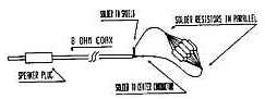
An injection probe is a coax that connects to your SSG, has a 0.01uF capacitor on the center conductor of the coax, and a tip connected to the other end of the capacitor. The shield of the coax connects to a ground clip. Many electronic supply shops sale injection probes. If you decide to purchase one, make sure it contains a 0.01uF capacitor between the tip and center conductor of the coax (used to block D.C.). If you decide to fabricate your own cable, it can be done with a few simple parts as shown in Figure 1.
8 OHM load
An 8 ohm non inductive load is used to substitute the internal speaker on the transceiver. The load is connected to the external speaker jack for convenience. For the purpose of troubleshooting a faulty receiver, it is not necessary to purchase a precision 8 ohm resistor (also, precision resistors are inductive). Six carbon composite 47 ohm, 1/2 watt resistors connected in parallel make an adequate load. Figure 2 shows a typical 8 ohm load fabrication.
Suppose you are given a dB value from the level diagram and you want to know its equivalent voltage:
Example: Given 0.5 µV = 0 dBµ,   |    Example: Given 224 mV = 0 dBm,
Find the dBµ value of 55dBµ.     |    find the dBm value of -55 dBm.
                                 |
                                 |
                X                |                    X
  55 = 20 log -------            |     -55 = 20 log --------
                    -6           |                        -3
             .5 X 10             |                 224 X 10
                                 |
                X                |                    X
2.75 = 20 log -------            |   -2.75 = 20 log --------
                    -6           |                        -3
             .5 X 10             |                 224 X 10
                                 |
                        X        |                            X
antilog 2.75 = 20 log -------    |   antilog -2.75 = 20 log --------
                            -6   |                                 -3
                     .5 X 10     |                         224 X 10
                                 |
              -6                 |            -6
562.3 (.5 X 10  ) = X            |  398.7 X 10   = X
                                 |
        -6                       |            -6
281 X 10   = X                   |  398.7 X 10   = X
                                 |
281 µV = A                       |  398.7 µV = X
                                 |


                Japanese "SSG"                  American "SSG"

                -6dB ------------------------------ 0.25µV
                 0dB ------------------------------ 0.5µV
                 6dB ------------------------------ 1µV
                12dB ------------------------------ 2µV
                24dB ------------------------------ 8µV
                30dB ------------------------------ 15.8µV
                40dB ------------------------------ 50µV
                50dB ------------------------------ 158µV
                60dB ------------------------------ 500µV
                70dB ------------------------------ 1.58mV
                80dB ------------------------------ 5mV
                90dB ------------------------------ 15.8mV
               100dB ------------------------------ 50mV
               120dB ------------------------------ 0.5V

                   TABLE 1 (dB or dBu to V conversion)


             Japanese "SSG"                         American "SSG"

             -119dBm ------------------------------ 0.25µV
             -113dBm ------------------------------ 0.5µV
             -107dBm ------------------------------ 1µV
             -101dBm ------------------------------ 2µV
             -88.9dBm ----------------------------- 8µV
             -83dBm ------------------------------- 15.8µV
             -73dBm ------------------------------- 50µV
             -63dBm ------------------------------- 158µV
             -53dBm ------------------------------- 500µV
             -43dBm ------------------------------- 1.58mV
             -33dBm ------------------------------- 5mV
             -23dBm ------------------------------- 15.8mV
             -13dBm ------------------------------- 50mV
               0dBm ------------------------------- 224mV
               7dBm ------------------------------- .5V

                        TABLE 2 (dBm to V conversion)
 -   Kenwood models:

                TS-140   TS-440   TS-450   TS-680   TS-690   TS-711
                TS-721   TS-811   TS-850   TS-940   TS-950


                        KENWOOD RS-232 INTERFACE

                                                               ( P.C.)

                                                            DB-25S (DB-9S)

                        +---------------------+         +----- 7     (5)
                        ¦                     ¦         ¦
                        ¦           MAX-232   ¦        +++     6
                        ¦        + +-------+  ¦
              78L05     ¦   +--¦+--¦1    16+--+            +-- 5     (8)
             +-----+    ¦   ¦    + ¦       ¦               ¦
     +12V ---¦I   O+----+------¦+--¦2    15+--+            +-- 4     (7)
             ¦  G  ¦ ¦ +¦   ¦      ¦       ¦ +++   RxD
             +-----+ ¦ ---  +------¦3    14+------------------ 3     (2)
                ¦    ¦ ---       + ¦       ¦       TxD
                ¦    ¦  ¦   +--¦+--¦4    13+------------------ 2     (3)
                ¦    ¦  ¦   ¦      ¦       ¦
               +++   ¦ +++  +------¦5    12+--------+          1
                     ¦        +    ¦       ¦        ¦
                     ¦      +--¦+--¦6    11+-----+  ¦
                     ¦      ¦      ¦       ¦     ¦  ¦
                     ¦      ¦      ¦7    10+     ¦  ¦           ( RADIO )
                     ¦     +++     ¦       ¦     ¦  ¦
                     ¦             ¦8     9+     ¦  ¦         DIN
                     ¦             +-------+     ¦  ¦
                     ¦                           ¦  ¦          6
                     ¦                           ¦  ¦
                     +------------------------+  ¦  ¦      +-- 5 (RTS)
                                              ¦  ¦  ¦      ¦
                                    74LS04    ¦  ¦  ¦      +-- 4 (CTS)
                                   +-------+  ¦  ¦  ¦
                                   ¦1    14+--+  ¦  ¦  +------ 3 (/RXD)
                                   ¦       ¦     ¦  ¦  ¦
                                   ¦2    13+------------------ 2 (/TXD)
                                   ¦       ¦     ¦  ¦  ¦
                                   ¦3    12+-----+  ¦  ¦   +-- 1 (GND)
                                   ¦       ¦        ¦  ¦   ¦
                                   ¦4    11+--------+  ¦  +++
                                   ¦       ¦           ¦
                                   ¦5    10+-----------+
                                   ¦       ¦
                                   ¦6     9+
                                   ¦       ¦
                                +--¦7     8+
                                ¦  +-------+
                               +++
NOTES:
                                       u
                                 1           4


                                 2           3


    Pin 1 = MIC input

    Pin 2 = PTT (Push To Talk)

    Pin 3 = Ground

    Pin 4 = Ground
NOTE
                                       u
                                 5           1

                                       6
                                 4
                                             2
                                      3

    Pin 1 = MIC input

    Pin 2 = PTT (Push To Talk)

    Pin 3 =

    Pin 4 =

    Pin 5 =

    Pin 6 = Ground
NOTE u
1 7
2 8 6
3 5
4
Pin 1 = MIC input
Pin 2 = PTT (Push To Talk)
Pin 3 =
Pin 4 =
Pin 5 =
Pin 6 =
Pin 7 = Ground
Pin 8 = Ground
NOTE the TM-741E the TM-241E
ZDDDDDDDDDDDDDDDDDDDDDD? ZDDDDDDDDDDDDDDDDDDDDDD?
3 ZDDDDDD? 3 3 ZDDDDDD? 3
3 3 ptt 3 3 3 3 ptt 3 3
3 3switch3 3 3 3switch3 3
3 @DDDDDDY 3 3 @DDDDDDY 3
3 DD 3 3 DD 3
3 J1 3 3 J3 3
3 3 3 3
3 3 3 3
@DDDDDDDDDDDDDDDDDDDDDDY @DDDDDDDDDDDDDDDDDDDDDDY
             the TM-741E                      the TM-241E
        ZDDDDDDDDDDDDDDDDDDDDDD?         ZDDDDDDDDDDDDDDDDDDDDDD?
        3  ZDDDD?              3         3    ZDD?              3
        3  3    3              3         3    3  3              3
        3                      3         3                      3
        3  3 3  3 3  3 3  3 3  3         3  3 3  3 3  3 3  3 3  3
        3   O    O    O    O   3         3   O    O    O    O   3
        3   3    3    3    3   3         3   3    3    3    3   3
        3   3    3    3    3   3         3   3    3    3    3   3
        3                      3         3                      3
        3 1750  VFO   MR   PF  3         3 1750  VFO   MR   PF  3
        3                      3         3                      3
        3                      3         3                      3
        3Microphone T91-0398-XX3         3Microphone T91-0398-X53
        @DDDDDDDDDDDDDDDDDDDDDDY         @DDDDDDDDDDDDDDDDDDDDDDY
 The new function becoms:
            ^                                 ^
            3                                 3
            3                                 3
    default:call                              call
programable:PF4                               ----
The optional filters listed below are for a narrower bandpass. Some will have different input & output impedance, & some will require new mounting holes. Only one will require a component change.
| Model | Standard | Option | Installation |
|---|---|---|---|
| TR-2200DA | CFM-455E | CFR-455G | Just replace |
| TR-7200A | CFR-455F | CFR-455G CFS-455G |
Just replace Modify PCB mounting |
| TS-700A/S/SP | CFR-455F | CFR-455G CFS-455G |
Just replace Just replace |
| TR-7400A | CFR-455F | CFR-455G | Just replace |
| TR-7600/7625 | CFR-455F2 | CFL-455F CFR-455G |
Replace C101 470pF to .00uF Replace C101 with .001uF & modify PCB mounting. |
| TR-8300 | CFM-455R | CFM-455F | Just replace |
Specification
| Filter Model |
Part Number |
-3 dB Down Bandwidth |
-6 dB Down Bandwidth |
Bandwidth | Impedance In/Out |
|---|---|---|---|---|---|
| CFM-455E | L72-0025-05 | More than ± 5.5KHz |
More than ± 8KHz |
60dB ± 16KHz |
1500 ohm |
| CFR-455F | L72-0037-05 | ± 4.5KHz | ± 6KHz | 70dB ± 16KHz |
2000 ohm |
| CFR-455G | L72-0302-05 | ---- | ± 4KHz | 70dB ± 16KHz |
2000 ohm |
| CFS-455G | L72-0303-05 | ---- | ± 4KHz | 80dB ± 16KHz |
2000 ohm |
| CFT-455F2 | L72-0309-05 | ± 5KHz | ± 7.5KHz | 60dB ± 16KHz |
1500 ohm |
| CFL-455F | L72-0306-05 | ± 4.2KHz | ± 6KHz | 70dB ± 16KHz |
2000 ohm |
| CFM-455F | L72-0000-00 | ± 4.2KHz | ± 6KHz | ± 12 KHz | 2000 ohm |
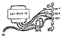
To operate the VFO-230 on 240V AC, the power transformer primary tap must be rewired from 120V to either the 220V or 240V tap.
Introduction
Kenwood service manual transmit level diagrams provide typical RF levels found in working transceivers. This information provides a fast method of locating a faulty circuit in a transmitter chain. To use the level diagrams, an AF VTVM, RF VTVM, and 50 ohm resistive load are required. In addition, since many units are tested with the drive output terminated into the load, a coax cable must be fabricated. A sample cable is shown below.
The transmit level diagrams are developed in a similar manner as the receive diagrams. Basically, a working transceiver is tuned for a specified output power at center frequency. The mic audio circuit is measured with an AF VTVM and the RF circuit is measured with an RF VTVM. The results are listed on the diagram as typical levels for a working transceiver. The exact setup used to make a diagram varies with the model. The setup details are listed in footnotes on the diagram. No matter what procedure is used, the end result is a list of typical levels for a working transceiver.
For the most part, variations in setup include what mode is used, if audio is applied to the mic input, and what reference is used for power output. Additionally, many units have the drive signal connected directly to a 50 ohm load. This requires a fabricated coax cable that can be inserted into the drive socket and attached to a load. A coax cable with a terminal that fits the drive socket is available in the Kenwood Parts Department. SB-905 lists the part numbers of coax cables that are available in several lengths and style. Once a cable is obtained, a connector that matches your 50 ohm load can be soldered to the cable.
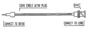
As mentioned above, certain units are terminated at the drive output. This procedure can be used in troubleshooting to determine if normal drive power is available. Simply connect the fabricated coax cable to the drive terminal and the 50 ohm load. If the load receives full drive power as indicated on the level diagram, the trouble spot is in the Final or LPF unit. In this case, reconnect the Final unit and continue checking towards the antenna terminal. If low drive is measured, continue measuring toward the mic input until a faulty circuit is found.
Once a faulty circuit is isolated, DC measurements must be made to determine
if normal supply voltage is present.
23-04-2000 Power
module heat sink compound
Author: Kenwood Communication, inc.
Symptom:
Several current and past model transceivers do not use
Heat Sink Compound on the power modules. Our engineering department determined
through testing, that those models with fine casting or machined areas under the
power module do not really require its use. Several service facilities and
customers have questioned this and are concerned that this could eventually
cause failure of the power modules(s).
Corrective Action:
In order to ameliorate any anxiety to increase
you confidence out engineers recommend that you use Silicone Heat Compound
whenever replacing any of these devices or whenever they must be lifted for
service of other components on the board. Our production lines begin using this
compound again as added protection for these devices.
Parts required:
Qty   Description                          New Part No.      Circuit Description
 1    Silicone Heat Sink Compound          W01-0411-05       NA