DTMF SQUELCH AND REMOTE CONTROL DECODER
This article describes how to build a general purpose DTMF decoder with a low-price chip from MITEL. The circuit supports DTMF squelch based on 3 digits station ID (full 999 combination). It also supports decoding of 4 additional commands - station ID plus one more digit which can be used to perform remote control on external devices (on/off or single shoot trigger operation ). One expansion port is included to provide future development.
Core of the whole equipment is the MT8870 DTMF decoder. This is a state of art single chip DTMF receiver incorporating "switched capacitor filter" technology and advanced digital counting / averaging algorithm for period measurement. Conventional method of frequency decoding usually based on frequency counting or phase locking technique. These methods are time consuming and inaccurate when handling unsteady complex signal. Switched capacitor filter technology based on a completely different approach. It works on the theory that any A.C. signal are rapid changes of potential energy with repect to specific time factor. A.C. components, provided that they bear the same frequency characteristic, will have the same timing on instantaneous potential variation. For example, a signal of frequency 1 Hz will experience peak positive value every one second. - the duration of 1 sec. will be constant among any A.C. signal bearing frequency 1 Hz, even though they have different wave forms.
Suppose a circuit is designed to sample the potential value of a signal at preset intervals ( say, at exactly 90 degree phase shift timing for a specific frequency ). If the total sum of all samples always experience zero while signal really present. We can conclude that an A.C. component of that specific frequency has been identified. Each fixed timing will be good for only one frequency. Since DTMF is a combination of 4 row tones and 4 column tones, it will need at least 8 sets of such time switching circuits. In the real world, there are more then 8 sets of such circuits in order to handle tolerance in the incoming DTMF signal while decoding result is developed on an averaging of outputs from all these filters.
Error detection control
There are two kinds of DTMF detection errors - TALKOFF and TWIST.
TWIST is the failure of decoding a valid DTMF signal due to non-linear frequency response of a transmission media. Among the two enemies, TWIST is easier to deal with since it can be controlled by audio equalization on the whole transmission path. These equalization can be done internally inside the DTMF decoding chip or externally via additional audio filters. According to factory specification, MT8870 can stand TWIST tolerance of +/- 6db. That is quite sufficient to compensate pre-emphasize and de-emphasize distortion caused by FM media. This should not be a problem unless the transmission is highly distorted.
TALKOFF is the wrong recognition of DTMF component in human voice as true DTMF signal. This is an unavoidable factor since human voice always contain valid DTMF combination. Fortunately, presence of these valid DTMF components are unsteady. Unlike real DTMF generated from a touch-tone keyboard, these 'human' DTMF cannot maintain on a constant combination. So they can be isolated by DELAY discrimination. If a decoded DTMF signal can stay on constantly for certain duration which exceed those normal period experienced in human voice, then it can be identified as a real DTMF command.
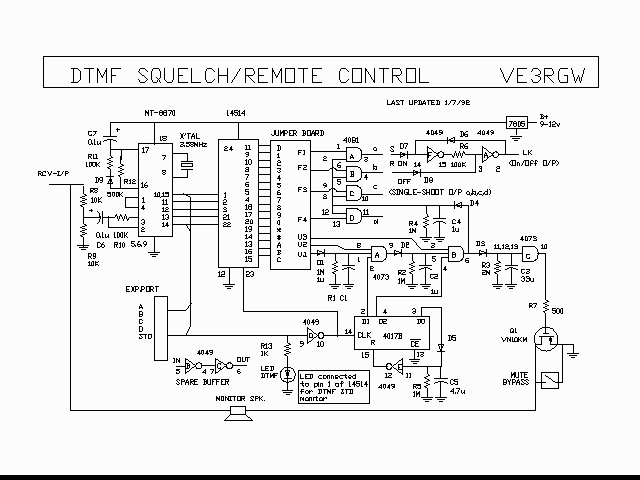
By looking at the schematic circuit, there are some external components hooked to MT8870 ( C2,R11,R12,D9 ). Pin 16 of MT8870 is EST (Early Steering) output. It will flag logic high whenever DTMF combination is detected in the input signal ( including TALKOFF error detection ). Pin 17 is GT (guard time) control, it is a trigger type input. The level on pin 17 is arranged as a delayed EST via C7 and R12. If the detection of DTMF is long enough for voltage at pin 17 to build up with time, it can be considered as a valid DTMF signal. The STD output line (pin 10) will flag logic high. Since it is connected to output data enable (pin 15), that will enable lines ( pin 11,12,13,14 ) to present numeric value of the decoded DTMF data. Yet, it takes the same delay for an RC circuit to discharge. That means TALKOFF detection can still occur in the following duration after a valid DTMF signal disappeared while C7 is still charged up. That is the reason of including D9 and R11. They are there to provide a fast discharge on C7 and ensure an immediate full delay guarding once a valid DTMF tone is gone.
Circuit Operation
The MT8870 monitors any audio coming from the receiver. The internal speaker of the receiver is muted while the external monitor speaker is switched by Q1 or a manual control bypass switch (Q1 is driven by the internal command decoding logic ).
The decoded BCD numeric data will carry a format as follows :
|
DTMF character |
Output data
D C B A |
|
D |
0000 |
|
1 |
0001 |
|
2 |
0010 |
|
3 |
0011 |
|
4 |
0100 |
|
5 |
0101 |
|
6 |
0110 |
|
7 |
0111 |
|
8 |
1000 |
|
9 |
1001 |
|
0 |
1010 |
|
* |
1011 |
|
# |
1100 |
|
A |
1101 |
|
B |
1110 |
|
C |
1111 |
These data will be decoded into16 individual outputs by the HEX decoder. Simply speaking if you got a DTMF "*" entry, you will get a logic high on pin19 from the 14514. All these16 outputs are connected to the program board which is only a 16 pin DIP IC socket. U1-U3, F1-F4 are input wires to the command decoding logic. The command programming is completed by jumping these wires into the corresponding pins on the program board. For example, if you want to program your station ID as number [ 330 ]. What you should do is just plug wire U1 to pin 3, U2 to pin 3 and U3 to pin 10 of the program board.
The command decoding logic is a bunch of gates combined with RC delay circuits. Thanks to the extra high input impedance of CMOS. That makes it is possible for an electric charge to stay at their inputs for hours until absorbed by a shunting resistor. Let's take one simple section as example. Look at the 4081 dual input gates, they formed a simple two digits command decoder. They are all connected to an RC circuit formed by R4 and C4. This RC will form a delay of about 1 sec. That is to say, if there has been a logic high coming through D4 , C4 will keep the charge and R4 will absorb them (discharge) to a logic low level within 1 sec. If another logic high is received on the second input ( F1-F4 matches a selected DTMF tone received ) before discharge completed, the concerned gate will open and a logic high appears at the output. This output can be used to drive external circuits. To change the intended delay for the waiting duration, just change RC, the larger R or C, the longer the waiting delay on the second digit.
One factor which affects accuracy of these timing is humidity within surrounding atmosphere. Such effect will be further emphasized if R value is high ( say exceeding 5M ohm ). Delay longer then 120 sec. is thus not recommended although it can be approached ( typical value for a 120 sec. delay is 5M / 47uf ). Tantalum capacitors are chosen due to the point that they are small in size and are enclosed in a better package. They can with stand higher changes of temperature and humidity.
Now let's look into the command decoder in more detail. U1,U2,U3 are programmed as the station ID number. The 4017 is a decade counter here equipped with auto-reset ability ( via D5,R5,C5,inverter E ). The D0 is output of decade stage 0, it will stay logic high as long as the counter stays idle. C5 is charged up continuously until the first DTMF entry is detected. That causes the counter to step-up by one, D0 will go logic low status while D1 will now be on logic high. Once that happen, charge at the input of inverter E will be discharged by R5 and approaches logic low within 3 sec. In this 3 sec. period, the counter can still count DTMF activities and moves the logic high status from D1 to D2 if a second DTMF tone is detected. Once the 3 sec. passed, the 4017 will reset and all command entries has to start from first digit again.
If the first digit of the DTMF entry is correct ( matches U1 ), two inputs of the 4073 will be on logic high ( supplied by 4017 D1 output and charged up C1 ). If the second digit of DTMF entry is also correct ( matches U2 ), output of 4073/section A will goes logic high and charges up C2. At the same time, since 4017 will move the logic high to its D2 output, the 4073/section B is now ready to decode the third DTMF digit - U3.
If a logic high is received from U3 within 1 sec. also, a logic high will be presented from 4073/ section B and charge up two following circuits. First circuit being a 45 sec. delay formed by 4073/section C (just a buffer ). The output of which will drive transistor Q1 and activates external speaker until time-out. That is how DTMF squelch being un-muted by detecting of the station's ID. Second circuit are those 4081 dual input gates mentioned previously. They are connected as additional remote control command decoders. Once station ID plus one more matching DTMF digit received ( programmed by F1,F2,F3,F4 ), the output of the corresponding 4081 will turns logic high while external devices can be triggered via output points (a,b,c,d). One special section is provided by the HEX inverters. Section A and F for the 4049 are connected as a toggle flip flop. If a logic high is received on the [on] input, the output will stay logic high until another logic high is received on the [off] input. This is just an example on how to construct a self locking on/off control circuit. One can connect output [a] to [on] and output [b] to [off] in order to program the [on] command as [ station ID + F1 ] while the [off] command be [ station ID + F2 ]. More control can be obtained in the same manner just by adding similar circuits.
If any error occurred in the command sending sequence, the counter will prevent further decoding immediately until the self-reset function is executed. So any command must be entered correctly within 3 sec. after a start, while there should be no hesitation of more then 1 sec. between any two digits. Else decode will fail due to time out. With such digit by digit checking , repeat numbers can be used consecutively in the station ID except that digit F1,F2,F3,F4 should not be the same as U3 else the 4th digit for that command will be ignored. The command circuit will fire after reception of the station ID since the whole 4 digits command is already received even though the use has not yet sent his 4th DTMF tone
Since only 4 units in the 4049 hex inverter are in use, the two spare units are connected in series ( on the PCB ) as a spare non-invert buffer. This can be used for future expansion or making the LED monitor to become a high impedance logic probe. Such simple device is very useful for diagnostic work at the construction stage. As shown in the circuit diagram, the LED is connected to show DTMF detection while the 4049 buffer is left vacant. User can determine their own need and change the connection accordingly.
Talking about quality of the un-muted audio. Transistor Q1 is driven from a relatively low voltage ( Vcc 5V plus lost due to current limiting of the 4073 output stage ). The un-muted audio will not be as natural as compared to that when bypass switch is on ( speaker connected to ground directly instead of via Q1). It will be sharper and slightly metallic in feeling. Using a relay to do the switching will solve the problem completely but that implies an increase in both cost and power consumption. Since one have to switch on the bypass switch as long as continuous communication is intended, the audio problem for the electronic switch is not so important.
One 3.579MHz color burst crystal is used as timing reference. That keeps DTMF decoding accuracy steady as a rock.
More detail of this article can be found in 73 Amateur Radio Today June 1992.