 |
|
|
|
|
The article is divided into two sections. Section A deals with typical CRO waveforms which might indicate certain characteristics or fault conditions in the electronic equipment being tested. The section shows various waveforms associated with square wave testing, sine wave testing, measurement of rise time and overshoot and measurement of phase shift. This section is part of the article "Measurement of Distortion" published in Amateur Radio, June 1989 (ref.1).
Section B displays Spectrum Analyser waveforms for sine wave, square wave, triangular wave and modulated signals. Also displayed are typical spectrograms made to measure frequency response or the characteristics of filters. This section was originally published in Amateur Radio, September 1987 (Ref 2).
)
SQUARE WAVE TESTING
One method of assessing frequency response (and sometimes other characteristics) is to feed a square wave to the input of the device under test and examine its output on a CRO. The square wave is made up of a fundamental frequency and all odd harmonies, theoretically to infinity. A deficiency within the frequency spectrum, from the fundamental upwards, will show a change in the shape of waveform. The test is subjective rather than precise but gives a good indication of the response.
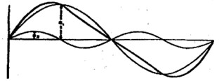
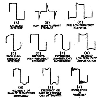 | Figure 1: Typical Square-Wave Response Patterns (A) Excellent Response (B) Poor Low Frequency Response (C) Fair Low Frequency Response (D) Poor High Frequency Response (E) Improved High Frequency Response (F) Emphasised Low Frequency Amplification (G) Reduced Low Frequency Amplification (H) Frequency or Band of Frequencies Emphasised (I ) Frequency or Band of Frequencies Attenuated (J) Oscillation or "Ringing" |
Typical response patterns taken from a reference source are shown in figure 1. The captions under the patterns decribe the various operational conditions and the effect of loss of low or high frequency response is illustrated. Further patterns shown in figure 2 also illustrate the effect on the waveforms when relative phase delay is changed over part of the frequency spectrum. Also observe in figure 1(J) how the ringing from oscillation in the circuit under test is initiated by the steep edge of the square wave. This is a test result on how the circuit might handle a transient which might not have been detected in carrying out a sine wave frequency response check.
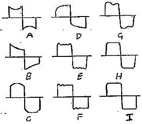
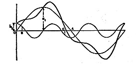
| Figure 2 - Typical Square-Wave Response Patterns (A) Deficient in Low Frequency, No Phase Error (B) Deficient in Low Frequency, Phase Advance (C) Excess Low Frequency, No Phase Error (D) Excess Low Frequency, Phase Delay (E) Deficient in High Frequency, No Phase Error (F) Deficient in High Frequency, Phase Delay (G) Sharp Cut-off above Square Wave Frequency (H) Gradual Cut-off above Square Wave Frequency (I) Gradual Cut-off at higher frequency than (h) |
Related to frequency response, there is a specification called "transient response' which is the ability of a device to respond to a stop function. "Rise time" is one measure of transient response and is the time taken for the signal, initiated from a stop function, to rise from 10 percent to 90 percent of its stable maximum value. Another measure is the percentage of the stable maximum value that the signal over-shoots in responding to the step. Figure 3 shows how the square wave, in conjunction with a calibrated CRO, can be used to measure rise time and overshoot.
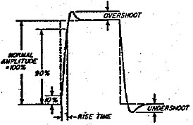 |
| Figure 3 - Transient Response - Measurement of Rise Time and Overshoot |
Rise time is also measure of the maximum slope of any sine wave component and hence is directly related to the limits in high frequency response. Together, rise time and overshoot define the ability of a device to reproduce transient type signals.
Another specification commonly used in operational amplifiers is the 'slew rate" given in volts per microsecond. Such amplifiers have limitations in the rate of change that the output can follow and this is defined by the slew rate. The greater the output voltage, the greater is the rise time and hence the greater the output voltage, the lower is the effective bandwidth. Slew rate is equal to the output voltage step divided by the rise time as measured over the 10 percent to 90 percent points, discussed previously. It is an interesting observation that, in specifying frequency response, output voltage should also be part of the specification.
HARMONIC DISTORTION
Harmonic distortion in any signal transmission device results from non-linearity in the device transfer characteristic. Additional frequency components, harmonically related to frequencies fed into the input, appear at the output in addition to the reproduction of the original input components.
Measurement of harmonic distortion can be carried out by feeding a sine wave into the input of the device and separating the sine wave from its harmonics at the output. Distortion is measured as the ratio of harmonic level to the level of the fundamental frequency. This is usually expressed as a percentage but sometimes also expressed as a decibel. Distortion Meters and types of distortion are described in the original article (Ref 1). Intermodulation distortion is described in ref 3.
SINE WAVE TESTING
Subjective testing for harmonic distorton can be carried out by feeding a good sine wave signal into the device under test and examining the device output on a CRO. Quite low values of distortion can be detected in this way.
 |
and Second Harmonic Frequency (a2). |
Some idea of the order of the harmonic can often be determined from the shape of the waveform. Figure 4 illustrates the formation of a composite waveform from a fundamental frequency and its second harmonic at one quarter of the fundamental Amplitude. Figure 5 illustrates similar formation from a fundamental frequency and its third harmonic, also a quarter of the fundamental amplitude. In Figure 5(b), the phase of the harmonic is shifted 180 degrees to that in Figure 5(a), and in Figure 5(c), the phase is shifted 90 degrees to that in (5a). The figures show that the composite wave forms can be quite different for different phase conditions making resolution sometimes tricky.
 | |
 | |
Diagrams (a), (b) & (c) show different phase relationships between harmonic and fundamental. |
Some distorted waveforms directly indicate an out of adjustment or incorrect operating condition. The clipped waveform of Figure 6(a) shows the output of an amplifier driven to an overload or saturated condition. Figure 6(b) is clipped in one direction indicating an off-centre setting of an amplifier operating point. Figure 6(c) shows crossover distortion in a Class B amplifier.
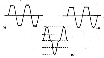 | Figure 6 - Distortion Waveforms. (a) Amplifier Overdriven. (b) Amplifier Operating Point not centered. (c) Crossover Distortion in Class B Stage. |
Another method of testing, using sine waves, is to feed the monitored device input signal to the X plates input of the CRO and the device output signal to the Y plates input of the CRO. This plots the transfer characteristic of the device, that is, instantaneous output voltage as a function of instantaneous input voltage. X and Y gain is adjusted for equal vertical and horizontal scan. A perfect response is indicated by a diagonal line on the screen, or with phase shift, an ellipse or circle. Figure 10 shows various fault wave forms taken from one reference source. The different effects are explained in the diagram captions.
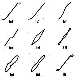 | Figure 7: Sine Wave Testing with Amplifier Input and Output fed to X and Y Plates of CRO, respectively (a) Amplifier Overdriven (b) Anode Bend Distortion in Valve Amplifier (c) Curvature Distortion (d) Crossover Distortion in a Class B Output Stage (e) Magnetising Current Distortion (f) As (e) with Phase Distortion later in the Chain (g) As (d) with Phase Distortion earlier in the Chain (h) As (c) with Phase Distortion earlier in the Chain (i) As (a) with Phase Distortion later in the Chain |
The same connection can be used to measure phase shift between two sine wave signals of the same frequency such as measuring the phase shift between the output and input of an amplifier. Typical measurements are shown in Figure 8. A straight forward sloped diagonal line indicates no phase shift. A straight reverse sloped diagonal line indicates 180°. A circle indicates 90° and an elipse 45° or 135°.

|
| Figure 8 - Measuring Phase Difference between two voltages of the same frequency. |
If a dual trace CRO is available, the two signals can be displayed together, one on each vertical or Y trace with normal X sweep. In this case, it is simply a matter of scaling off the phase difference along the Y axis graticle.
Over the years, the cathode ray oscilloscope (CRO) has been a universal instrument for examining analogue signals. Rapid advances in technology have led to a era of microcomputer controlled, digitally controlled test equipment, not the least of which is the modern spectrum analyser which enables greater precision analysis of analogue signals than is possible with the CRO. A spectrum analyser plots signal amplitude (or signal power) as a function of frequency compared to the CRO which plots signal amplitude as a function of time.
The spectrum analyser is not the type of equipment normally within the reach of the radio amateur and because of this, it was thought that it would be of interest to illustrate a few spectrum plots of well-known waveforms.
BASIC WAVEFORMS
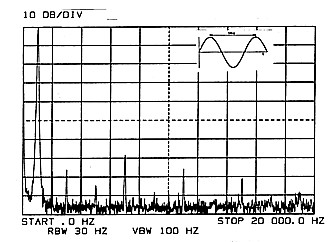
Figure 1 shows the spectrum of a sine wave oscillator with fundamental at 1000 Hz and harmonics up to 20 kHz. The highest level harmonic at 7 kHz is 70 dB below the fundamental, representing a harmonic distortion of 0.03 percent. This is a very good oscillator which would not be matched by many laboratory instruments. It can also be seen that the noise floor is about 95 dB below the fundamental and this is also very good. The oscillator noise level might be even better than this as much of the noise is due to the spectrum analyser itself.
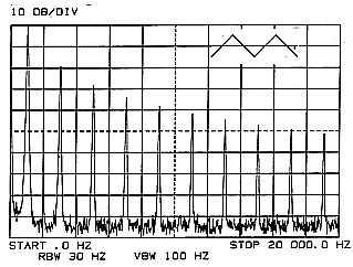
Figure 2 shows a 1000 Hz square wave. A perfect square wave generates odd harmonics to infinity with an amplitude 1/n relative to that of the fundamental or (20 log n) dB below the fundamental. ('n' is the order of harmonic). For n = 3, 5, 7 and 9 this calculates to -9.5, -14, -16.9 and -19.1 dB respectively, very close to the readings shown in Figure 2.
 |
 |
1000 Hz Sine Wave and Harmonics. | 1000 Hz Square Wave Showing Harmonics to 20 kHz. |
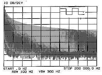
Figure 3 is the same square wave plotted out to 200 kHz and showing the apparently unlimited spread of harmonics. From this, it is easy to see why a low frequency square wave oscillator can be used as a marker generator over a wide frequency range.
Figure 4 shows a 1000 Hz triangular wave. A perfect triangular wave also generates odd harmonics to infinity, but each amplitude is (l/n) squared relative to the fundamental or (40 log n) dB below the fundamental. For n = 3, 5, 7, and 9, the calculation is -19, -28, -33.8, and -38.2 dB respectfully, again very close to the readings shown.
 |
 |
showing harmonics to 200 kHz |
MODULATION
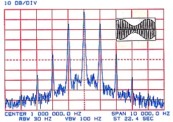
Figure 5 shows a 1 MHz carrier frequency, amplitude modulated by a frequency of 1 kHz to a modulation depth of 50 percent. For this case, the two side frequencies, 1 kHz either side of the carrier, are 12 dB below the carrier level, or a quarter of its amplitude. Other side frequencies at 2 kHz and 3 kHz, either side of the carrier, are the result of harmonics either in the original modulating tone or distortion caused by the modulation process. The 2 kHz side frequencies are about 30 dB below the 1 kHz side frequencies representing about three percent distortion in the system.
In Figure 6, the modulation level has been increased to 100 percent and the side frequencies, 1 kHz either side of the carrier, are now 6 dB below carrier level, or half its amplitude. The spectrum has been expanded to show many more harmonically related sideband components which now appear. Except for those close to the carrier, most of the components are more than 50 dB down and not of any great concern.
 |
 |
- Modulating Frequency 1000 Hz. | - Modulating Frequency 1000 Hz. |
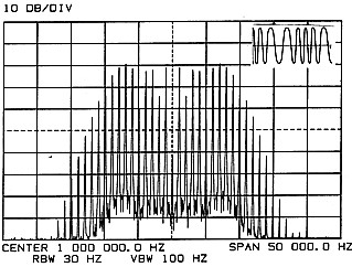
In Figure 7, the carrier is over-modulated and there is now a spread of sideband components about 30 dB down. If this were an amateur radio transmitter, other amateur stations in nearby suburbs would be complaining about sideband splatter.
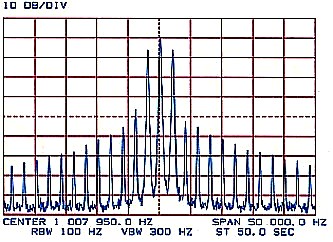
Figure 8 Shows a 1 MHz carrier, frequency modulated by a 1 kHz tone with a deviation of 8.650 kHz, representing a modulation index of 8.650. It can be seen that there are many side frequencies all spaced by an amount equal to the modulating frequency (1 kHz). For this signal, a significant bandwidth of about 20 to 30 kHz is being utilised.
 |
 |
- Modulating Frequency 1000 Hz. | - Modulating Frequency 1000 Hz. - Modulation Index 8.650 and showing Third Carrier Null. |
If we now examine Figure 9, which plots the amplitude of the carrier and side frequencies against the value of modulation index, we can see that there are a number of values of modulation index where the carrier level becomes zero. These are very convenient references to calibrate the amount of deviation. In Figure 8, the deviation has been set to produce the third carrier null at a modulation index of 8.650, so we know precisely that with our modulating frequency of 1000 Hz, our deviation is 8.650 x 1000 = 8850 Hz.
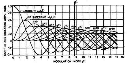 |
(Third carrier null at modulation index = 8.650) |
FREQUENCY RESPONSE
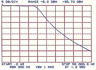
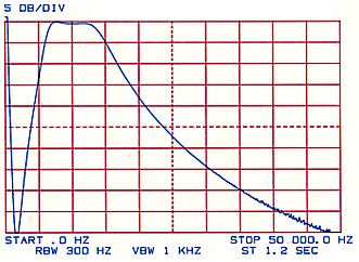
Another useful function of the spectrum analyser is to plot the frequency response of a four terminal device such as an amplifier or a filter. In this case, the analyser frequency sweep generator is fed to the input of the device and the output of the device is fed to the input of the analyser. Typical plots of a low pass filter and a bandpass filter are shown in Figures 10 and 11 respectively
 |
 |
REFERENCES
(1) Measurement of Distortion - Lloyd Butler VK5BR - Amateur Radio, June 1989.