
|
Introduction
Output impedance is a term commonly used by manufacturers in the specification of the output circuit in electronic equipment such as amplifiers and transmitters. What they usually mean is that this is the load impedance into which the equipment is designed to operate. There seems to be a lot of confusion about the term output impedance as it is often taken to mean, and often meant to mean, the source impedance of the equipment. In precision test equipment, the design is such that the source impedance is made equal to the load impedance into which it is meant to operate. However, in other equipment the source impedance is usually quite different from the load impedance used and it seems that this is not always appreciated.
In the following paragraphs, we will examine the characteristics which define source resistance and load resistance for valve and transistor power amplifiers.Hopefully, we might be able to clear up a few questions, often misrepresented concerning amplifier output circuits. In the discussion which follows, the word resistance will sometimes be substituted for impedance in the explanations which are given. For the purposes of the discussion, the impedances will be considered as resistive. To eliminate confusion, the term output impedance will also be avoided.
Matching
The idea of matching load impedance to source impedance stems from a principle shown in figure 1 in which a generator supplies power to its load (RL) via its own internal or source resistance (Rs). If we commence with RL greater than Rs, more power will be dissipated in RL than in Rs. As we decrease RL, the power in both RL and Rs will increase up to the point where, RL = Rs and equal power will be dissipated in each. Decreasing RL further increases the power lost in Rs but the power in RL is decreased. Clearly, maximum possible power is dissipated in RL when RL = Rs.
|
|
The problem with this matching system of RL = Rs is that half the power is lost in the source. Imagine a power supply authority tolerating a system in which half the power they generate is lost in their own generating machines. The best system, from their point of view, is one in which Rs is the lowest. In the valve or transistor amplifier, the problem is not quite the same and this will be discussed further on.
A concern with matching in amateur radio is the prevention of signal reflections on our transmission lines. Reflections occur on a transmission line if the line is not terminated in a resistance equal to its characteristic impedance, or if an impedance discontinuity occurs along the path of the line. Reflections on the line cause standing waves which increase line loss and in the case of pulse or video type signals, degrade the quality of the signals.
Let us now consider the source impedance of the transmitter feeding the transmission line. If there are reflections on the line, the reflected signals are returned to the source. If the source impedance is equal to the line impedance, the reflected signals will be absorbed by the source. On the other hand, if there is a mismatch here, the reflected signals will be further reflected back down the line to aggravate the standing wave condition. So here is a good reason for the source impedance to be matched to the transmission line impedance.
Suppose we have a transmission line which is correctly matched and has no reflections on the line, or alternatively, there are standing waves but these are made invisible to the transmitter by inserting a matching network or aerial tuner between the transmitter and the line. In this case, there is no reflected signal to be absorbed or re-reflected and as far as standing waves are concerned, it does not matter one iota what source impedance is seen in the transmitter With this considered, perhaps the source impedance of the transmitter is not so important after all. Our main concern is that the specified load impedance (usually 50 ohms resistive) is reflected across the transmitter output from the transmission line load.
In the paragraphs which follow, source resistance and load resistance will be examined using valve and transistor characteristic curves to show how these two parameters are likely to be widely mismatched. To demonstrate the arguments which will be submitted, the amplifiers will be considered to operate essentially in Class A as this class of operation is more straightforward to analyse than classes which utilise plate or collector current flow over less than the full AC cycle.
Source Resistance
Source resistance of an amplifier is equal to the AC plate resistance (or collector resistance in the case of the transistor) divided by the impedance ratio of the output coupling circuit. For simplification of the discussion, impedance ratio of the output circuit will be taken as 1:1.
The plate resistance (Rp), at a given grid voltage (Ec), is the reciprocal of the slope of the plate current (Ib) versus plate voltage (Eb) curve. On the curves of figures 2 and 3, it is derived by taking the ratio of a change in Ib to a change in Eb for a constant Ec. In the beam tetrode case of figure 2, grid voltage (Ec) is set at -15V and plate resistance is derived as 50,000 ohms. In the triode example of figure 3, grid voltage is set at -12.5V and plate resistance is derived as 2,083 ohms. Observe the difference in slope between the tetrode and triode curves and the resultant much higher plate resistance of the tetrode than that of the triode.

|
|
Plate Resistance (Rp) = ΔEb/ΔIb [Grid Voltage(Eg1) is constant] = (350 - 150).1000/(52 - 48) = 50,000 Ω |

|
|
Plate Resistance (Rp) = ΔEb/ΔIb [Grid Voltage(Eg1) is constant] = (300 - 200).1000/(75 - 27) = 2083 Ω |
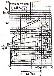
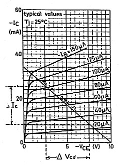
In the transistor example (figure 4), collector resistance (Rc) is the ratio of a change in collector/emitter voltage (Vce) to a change in collector current (Ic) for a constant base current (Ib). For a base current of 60 microamps, Rc is derived as 2,174 ohms.
 |
|
Collector Resistance (Rc) = ΔVce/ΔIc [Ie is constant] = (7.5 - 2.5).1000/(18 - 15.7) = 2174 Ω |
Load Resistance
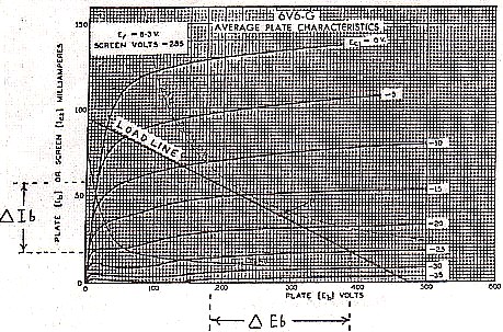
The reflected load resistance (RL) to the valve amplifier can be represented by drawing a load line on the Ib versus Eb curves (refer figures 5 and 6). The load line represents the swing of plate voltage and plate current under operational or dynamic conditions. Its slope is equal to -1/RL, where RL is the load resistance, or the ratio of a change in Eb to a change in Ib read along the load line in reversed sign.
 |
|
= -(385 - 185).1000/(18 - 58) = 5000 Ω |
 |
|
= -(320 - 180).1000/(30 - 66) = 3889 Ω |
The valve characteristic curves are far from perfect and the load line is set for a compromise which achieves as high as possible maximum power output consistent with an acceptable level of distortion. The load line must also lie within the limits of the maximum power dissipation curve. For the tetrode case shown in figure 5, the optimum load resistance is around 5,000 ohms.
Referring back to the derivation of plate resistance, we see that at 50,000 ohms, the plate resistance is ten times the load resistance. The plate resistance is seen by the load as the source resistance which, for the tetrode, is typically much higher than the load resistance.
Figure 6 shows a load line selected for the triode connected amplifier. In this case, the load resistance is 3,889 ohms and different from the tetrode, is higher than the plate resistance which was derived as 2,083 ohms. For the triode case, the source resistance at the amplifier output is typically lower than the load resistance.
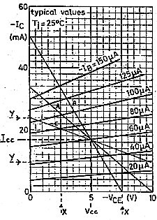
Finally, figure 7 shows a load line drawn for the transistor. With the operating point set for a supply voltage (Vcc) = 5V and a base current (Ib) = 60 micro-amps, the line is drawn from the X axis, at a value of Vce equal to twice Vcc, through the operating point, to the Y axis scaled Ic. The load resistance is equal to the ratio of a change in Vc to a change in Ic along the load line in reversed sign The load resistance is derived as 294 ohms and much like the tetrode, is a much lower value of resistance than that derived for the collector resistance, or source resistance of 2,174 ohms.
 |
|
[Along the load line] = 294 Ω |
The examples illustrate the general relationship between source resistance and load resistance in valve and transistor power amplifiers. For tetrode valve and transistor amplifiers, the source resistance is very much higher than the load resistance. The pentode valve is also much the same as the tetrode in this respect.
The triode valve is different. For this amplifier, the source resistance is normally lower than the load resistance. For class A triode power amplifiers, the load resistance usually works out to be around two to three times the plate resistance.
Efficiency
The amplifier stage is often depicted using the analogy of figure 1, of an AC generator in series with its own plate or collector resistance, connected to the load. This is a very useful analogy to calculate such factors as stage gain, but if we use it to calculate efficiency, the analogy fails. When we apply it to the tetrode or pentode valve or the transistor amplifier, each of which have high AC source resistance compared to the load resistance used, we see a condition in which most of the power generated appears to be lost within the source resistance of the amplifier. This condition is not true.
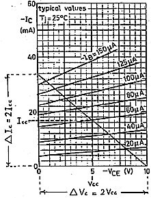
It can be shown that, for an amplifier with ideal characteristic curves, maximum efficiency class A is 50% and maximum efficiency class B is 78%. The transistor efficiency closely approaches these values, limited essentially by the bends in the curves at low collector voltage and which are clearly seen in figures 4 and 7. To Illustrate the class A case, we will pretend the bends in the curves are not there as shown in figure 8. DC power is given by the product of collector supply voltage (Vcc) and the average collector current (Icc) i.e. Pdc = Vcc.Icc
Maximum AC voltage swing is twice Vcc and maximum AC current swing is twice Icc. To get RMS values we divide both of these by 2√2 and the product of the two results is AC power, i.e.
Pac = 2Vcc.2Ic/ (2√2).(2√2)
= (4Vcc.Icc)/8
= (Vcc.Icc)/2
The AC power is clearly half the DC power and the maximum efficiency is 50%. It should be observed that this calculation is unaffected by the slope of the Ic versus Vc curves, and hence, unaffected by the high value of collector resistance. For our amplifier, the circuit analogy of figure 1 cannot be used to calculate efficiency of the stage.
It is interesting to observe that, when Vc is maximum, Ic is minimum and when Vc is minimum, Ic is maximum. In other words, the AC current swing is 180 degrees out of phase with the AC voltage swing. This is exactly opposite to power consumed in a resistance and hence we can consider the amplifier as a negative resistance or a generator of power.
Maximum Power Output & Power Sensitivity
 |
| |
|
Fig 8. Idealised transistor curves and maximum power output. |
Fig 9. Effect of changing load resistance from optimum value. |
At this point we will examine the optimum value of load resistance. Maximum power output is achievable when the load line intersects the Vc axis at twice Vcc, as shown in figure 8 and as curve A in figure 9. If the load resistance is reduced so that we get curve B in figure 9, the voltage swing is limited to that shown by XX. If the load resistance is increased so that we get curve C, the current swing is limited to that shown by YY. In either case, the maximum power output is less than that achievable with curve A. All this leads to the well known formula:
Load resistance (RL) = Vcc²/2Po
Where theoretical maximum power (Po)
= Power input/2
= (Vcc.Icc)/2
Maximum power output should not be confused with power sensitivity which is the ratio of power output to the input signal power to the base. It is equal to: (ΔIc)².RL/(ΔIb)² (along the load line) or approximately (Hfe)².RL where Hfe is the transistor current transfer ratio and collector resistance (Rc) is much greater than RL.
Power sensitivity is increased as RL is increased but, of course, at the expense of lower maximum power output.
Although the amplifier generates AC power, it is not quite the same as an alternator source. It is really a direct current device in which the circuit DC resistance and hence the circuit current, is made to change by changing the input base current, or in a valve, the grid voltage. By feeding an AC signal to the input, an AC current component is superimposed on the direct current. The AC is separated from the summed result by capacitive or transformer coupling.
In other respects, the amplifier behaves like an AC source. The source resistance can be considered to be what a signal would see if fed backwards into the amplifier output. (For example, the reflected signal returned on a transmission line or the signal generated by resonance in a loudspeaker following an impulse or transient). In this case, the backwards signal voltage attempts to vary the amplifier current and in the transistor, the collector current tends to remain near constant resulting in a high reflected AC resistance.
As pointed out before, the analogy of figure 1 is not relevant to calculation of maximum power output or power efficiency but it certainly can be used in the derivation of stage gain and power sensitivity. An example of its use is the well known formula for stage gain in a triode valve amplifier:
Stage gain (A) = μRL/(RL + Rp)
where μ = amplification factor
Making use of figure 1, the generator voltage is equal to the AC input voltage multiplied by the amplification factor. Of course stage gain can also be directly read from curves such as those shown for the triode, in figure 6. In this case, stage gain is equal to the ratio of change in Eb to change in Ec read along the load line.
Negative Feedback
We have shown that source resistance in an amplifier can be quite different from the load resistance used, but often there is a need to change it so that Rs equals the load resistance or some other desired value. For example, in a moving coil loudspeaker there is a need for heavy damping to prevent the speaker cone resonating when a transient is delivered. This can be done, without loss of speaker efficiency, by feeding the speaker from a low resistance source which acts as an electrical load to damp out the resonance.
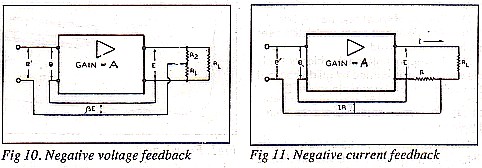
Negative feedback is commonly applied to amplifiers to reduce distortion and noise generated within the amplifier itself. It is also used to modify the amplifier source resistance. Negative feedback can be categorised into negative voltage feedback and negative current feedback.
Negative voltage feedback is defined as voltage fed back to the amplifier input in proportion to the voltage across the output load (refer figure 10). Negative current feedback is defined as voltage fed back to the amplifier input in proportion to the current through the output load (refer figure 11). Voltage feedback decreases the effective source resistance whilst current feedback increases it. By applying a controlled amount of voltage or current feedback (or a combination of both), the source resistance can be modified to a selected desired value.
|
Whilst negative feedback is common in audio frequency power amplifiers, it is difficult to apply where there are loads which become reactive at certain frequencies and cause sufficient phase shift to make the feedback positive and the amplifier unstable at these frequencies. Because of this, negative feedback is not a proposition in tuned RF amplifiers and in these, we must accept the inherent plate resistance or collector resistance to define source resistance.
Class B
Preceding examples of amplifiers have operated in class A, so we will extend the exercise to examine the relationship between source resistance and load resistance for class B. In class B operation, the amplifier is biased for near plate current or collector current cut off and current flows for half of the AC cycle of signal output. The other half cycle is provided by a second amplifier to make a push-pull circuit, or in a tuned RF amplifier, can be provided by the inertia or flywheel effect of the tuned tank circuit.
Class B operation is discussed with reference to the transistor curves of figure 12. For zero signal, the collector voltage is equal to the supply voltage (Vcc of 7.5V) and collector current (Ic) is near zero. Maximum current swing on load line A is limited to the point where the load line intersects minimum collector voltage on the Ic versus Vce curves.
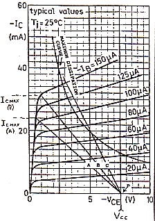
|
Maximum current swing and maximum power output can be increased by decreasing the value of load resistance (RL) as shown in load line B. Further decrease of load resistance (load line C) further increases the maximum current and maximum power output but the load line now crosses the maximum power dissipation curve set on the diagram for 100mW. Maximum power output is thus achieved with a load line which is drawn from a point at Vcc and Ic = 0 to just within the limits of the power dissipation curve.
As can be seen from the diagram, the absolute value of the negative going slope of a typical load line is much greater than the slope of the Ic versus Vce curves and hence, the value of load resistance is again much smaller than the value of collector resistance, probably oven more so than for class A.
If two transistors are used in class B push-pull and their curves are assumed to be ideal with no bottoming voltage, at maximum power output, peak to peak voltage swing is 2Vcc and peak to peak current swing is 2Icmax. From this information we can calculate maximum theoretical efficiency. Rms values are derived by dividing the peak to peak values by 2√2. Maximum power output is calculated from the RMS values as follows:
Po = (2Vcc).(2Icmax)/ (2.√2)²
= 0.5 Vcc.Icmax
The DC current input to the stage looks like a full wave rectified signal and hence the average current is well known as 0.636 of the peak value so that DC input power is calculated as 0.636Ic.Vcc. Clearly, power efficiency is the ratio 0.5/0.636 which evaluates to 78'%.
Once again, we see that our collector resistance or source resistance does not enter the calculation and the fact that source resistance is higher than load resistance is of no consequence to the power efficiency and maximum power output.
We could go on to discuss class C but the examples already presented should be sufficient to support the arguments presented. Field effect transistors have also not been discussed, but it is sufficient to say that their drain current versus drain to source voltage curves are much the same sort of shape as those of the bipolar transistor resulting in much the same high source resistance.
Summary
In setting out the arguments, the text has aimed at demonstrating the following:
(1) The term output impedance can mean source impedance or source resistance, but it is often meant to imply operational load impedance. In our discussion, we have avoided confusion by referring only to source resistance or load resistance.
(2) In tetrode and pentode power amplifiers and in transistor power amplifiers, the source resistance is normally much higher than the load resistance. In triode power amplifiers, the source resistance is lower than the load resistance.
(3) Because of the above, impedance match between the RF power amplifier source and the connected transmission line is most unlikely. Providing the transmission line load is matched for a low standing wave ratio at the transmitter output and it presents a resistive load to the transmitter equal to that for which the transmitter is designed, the mismatch of transmitter source resistance to its load is of little consequence.
(4) The fact that the transmitter source resistance is higher than the load resistance, as in the pentode, tetrode and transistor, does not limit power transfer efficiency or maximum power output as would occur if the high source resistance were inherent in a simple generator.
Although it was not the specific aim, discussion has demonstrated some of the useful applications of amplifier static characteristic curves and load lines. Without these curves, it would have been difficult to justify the various points that have been made concerning source resistance and load resistance.