VK3BIZ IC215 Synthesiser Project
IC215 Frequency Synthesiser
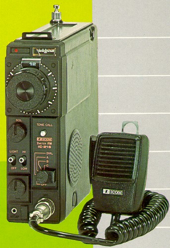
I have an old crystal locked IC215 2 metre portable radio which I thought I could update to include a frequency synthesiser rather than spending outrageous amounts of money buying crystals.
I have designed a Synthesiser circuit based on the ATMEL AT90S2343 8pin dip flash processor and the Motorola MC145159 Serial Phase Locked Loop. The board will be designed to fit into the radio where the crystals now reside.The channel switch on the IC215 has twelve positions and there are another 4 positions on the power switch for priority channels. These two switches can be used together by reconnecting the 12 position switch wiper to ground and the "Dial" line to a spare pin on the crystal switch plug. This can give 48 channels.
The IC215 uses three doublers on the transmit side. The crystal oscillator operates from 18.25MHz to 18.5MHz to cover the band from 146MHz to 148MHz. The receiver local oscilator uses two tripplers and is offset by 10.7MHz, so 146MHz TX corresponds to 135.3MHz/9 = 15.0333MHz and 148MHz TX => 137.3MHz/9 = 15.3222MHz.
If we assume a 25KHz channel spacing, the synthesiser reference frequency can be programmed to be 1/9th the channel spacing for receive or 1/8th the channel spacing for transmit, which gives a reference fequency around 3KHz. This makes programming the synthesiser a simple matter of adding or subtracting an offset to the TX synthesiser count for receive and simplex/ duplex offsets.
My thoughts on channel allocation went as follows:
Dial Ch1->Ch8 146.650->147.000 50KHz spacing (Duplex -600KHz)
Dial Ch9->Ch12 146.450->146.600 50KHz spacing (Simplex)
A Ch1->Ch8 147.050->147.400 50KHz spacing (Duplex +600KHz)
A CH9->Ch12 147.450->147.600 50KHz spacing (Simplex)
B Ch1->Ch8 146.625->146.975 50KHz spacing (Duplex -600KHz)
B Ch9->Ch12 146.425->146.575 50KHz spacing (Simplex)
C Ch1->Ch8 147.025->147.375 50KHz spacing (Duplex +600KHz)
C CH9->Ch12 147.425->147.575 50KHz spacing (Simplex)Synthesiser Design Note
The MC145159 used in this design is now obsolete. I only used it because I had a few of them left over in the junk box.. Click here for the Motorola Applications Note AN969 on the MC145159. Note that this file is about 1.5Mbytes long.The MC145159 is designed to operate up to about 15MHz at 5V although the typical operation goes up to 18MHz and I am relying on that to a certain extent. The upper frequency limit is determined by the drive level
into the sysnthesiser chip, but I am not sure at this stagewhat the drive level out of the VCO will be.The MC145159 has an analog phase detector, that requires a few Rs and Cs to be hung on it for the charge ramp and hold timing. When I did the loop filter calculations, with Delta Freq = 0.5MHz and Delta Control Voltage = VDD or 5V and a reference frequency of around 3 KHz the damping factor Sigma and the Natural Frequency of the Loop Wn were very high.
the phase detector gain Kphi = VDD/2 pi (VDD = 5V)
the VCO constant Kvco = 2 pi (Fvcohi - Fvcolo)/( Vvcohi - Vvcolo)
KvcoKphi = (Fvcohi - Fvcolo)Fvcohi = 18.5MHz Fvcolo = 18.0 MHz
Vvcohi = VDD = 5V Vvcolo = 0V
Fref = Channel Spacing / Frequency Multiplication = 25KHz / 8 = ~3KHzFor a single pole RC filter
Wn = sqr( KphiKvco/(NRC) )
Sigma =(N. Wn) / (2. KphiKvco)N = 146MHz / 25KHz = 18.5Mhz / 3KHz = 5840
RC = KphiKvco / N.Wm^2designing for Wn = 2 pi Fref / 10 = 2 . 3.1416 . 3000 / 10 = ~2000 radian
designing for Sigma = 1
Wn = 2. KphiKvco/ N = 2 . 500.10^3 / 5840 = ~ 200 radianobviously there is a big difference in the natural frequency of the loop filter.
The lock time of the loop can be pretty long (not time critical) so choose the lower value of Wn.
I think that means the loop will be more stable.RC = KphiKvco /( N. (2.KphiKVco/N) ^2 ) = N / (4. KvcoKphi )
RC = 5840 /( 4. 500 . 10^3) = ~ 6000 / 2. 10^6 = ~3. 10^-3if C = 10nF -> R = 330K
Circuit Description
The Circuit Diagram can be obtained in GIF form hereThe Synthesiser Circuit makes use of an Atmel ATS2343 Flash microprocessor that I got with the STK200 kit. I have provided the same interface header on it as is used in the STK200, so I can use the interface adapter from that kit to program the processor in circuit.
I am using the SPI serial interface on the chip with MOSI (Master Out Slave In) for the synthesiser and MISO (Master In Slave Out) for the switch interface. I am using PB3 for the Shift / Latch function on the serial shift registers and the synthesiser. PB4 is used for the PTT sense input. It is necessary to program the synthesiser at the same time that the parallel load shift registers are read.
On release from reset ( Q1 & Q2) the processor scans the position of the 12 position channel switch and the 5 position power / priority channel switch to encode a channel number. The sysnthesiser is initially programmed for receive, with a referency frequency of 25KHz/9. The PTTIN line is polled by the processor for TX requests. On PTT the reference divider is changed to 25KHz / 8.
I had an extra shift register in the design at one stage to test for PTT and Lock Detect with a PTT output on PB3, but I thought it was more reliable to AND PTT with the Lock detector (Q3, Q4 & Q5) to key the transmitter. It also reduced the component count.
Because the TX VCO frequency must be switched around 3 MHz higher than the RX VCO frequency, the PTTIN circuit shorts out an inductor in the VCO tank. I hope this works !!! I plan to use a small toroid for the two VCO inductors, so adjustment might be a little tricky. The turns ratio on the toroid may need to be adjusted by hand.
The AT90S2343 has 128bytes of EEPROM which should be plenty to hold the frequency information. ie. 2 bytes per channel. This could be a 14 bit division factor for RX as well as 2 bits for Simplex/Duplex and Duplex +/-. The RX and TX reference frequency for the synthesiser loop can be reprogrammed separately so the RX and TX division ratios are scaled accordingly. It should be a simple matter of adding an offset count for the receive IF and duplex offsets
Software will be posted as the project develops.