ON7YD
3.5MHz low power  ARDF transmitter
Partlist
| IC1 : CD4001 | X1 : 3.5..MHz | R1 : 1.5M | R2 : 330k | R3 : 330k |
| C1 : 100p | C2 : 100p | C3 : 5-60p | C4 : 470n | C5 : 330p |
| C6 : 47p | C7 : 100n | TR1 : * | | |
* TR1 : from my junk-box, 1/20 transformer ratio (more details see below)
back to top of this page
Functional description
General
This low power transmitter is developed for ARDF exercising purposes but of course can be used as super QRP transmitter either. With 1 or 2 meter wire as antenna and a ARDF receiver with ferrite-rod antenna the range is about 100m but with better antennas and a 'real' receiver the range is probably much larger.
Technical
All active elements of the transmitter are within a single CMOS IC (NOR gates). One gate (IC1D) is the xtal oscillator, C3 can be used to adjust the frequency a few kHz. With two other gates (IC1B and IC1C) a second oscilator is built (at a frequency of less than 1Hz) that is used to key the transmitter. R2, R3 and C4 determine the frequency of this oscillator. The remaining gate (IC1A) is used as keyed 'PA'. C5 decouples the DC from the output filter TR1 / C6. The antenna matching is done by the transformer-ratio of of TR1. The transmitter is tuned for maximum power by adjusting the core of TR1.
If used as a ARDF training transmitter a short wire of a few meter is sufficient and the transformer ratio is not critical (20/1 is a good value - with the IC1A at the low-impedance side).
If used with a larger antenna a lot of dB's can be won by experimenting with the tranformer ratio.
Construction
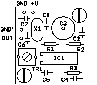
There is little to say about the construction. The only components that can be mounted wrong are IC1 and TR1. In case of TR1 this is non-destructive, you just won't get any power out of the transmitter, but in case of IC1 you most likely will have to replace the integrated circuit.
back to top of this page
Circuit diagram
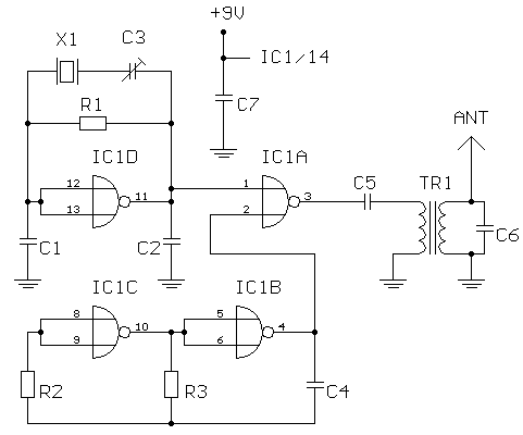 A high resolution TIFF file of the circuit diagram is included in the download package.
back to top of this page
A high resolution TIFF file of the circuit diagram is included in the download package.
back to top of this page
Printed Circuit Board
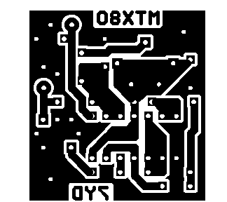
 The exact dimensions of the PCB are 2.0 x 1.5 inch (50.8 x 38.1 mm).
A high resolution TIFF file of the PCB is included in the download package.
back to top of this page
Download
Click here to download a ZIP-file that contains :
- high resolution Printed Circuit Board (TIFF file)
- PCB component layout (TIFF file)
- high resolution circuit diagram (TIFF file)
- complete functional description and manual (WORD document)
- terms of usage and disclaimer (ASCII file)
back to top of this page
You are visitor number  since 21 feb. 2000