PIC Frequency Counter with Frequency Lock functionWritten by: OH6CJ Osmo, January 13th, 2002, E-mail: [email protected] |
||||||||||||||||||||||||||||||||||||||||||||||||||||||||||||||||||||||||||||||||||||||||||||
|
||||||||||||||||||||||||||||||||||||||||||||||||||||||||||||||||||||||||||||||||||||||||||||
|
This PIC software combines frequency counter and frequency lock functions. By adding couple of transistors and operation amplifier TL082, it is possible to lock the LC oscillator frequency. Let’s look at the following block diagram. Software functions are presented inside the dashed area. 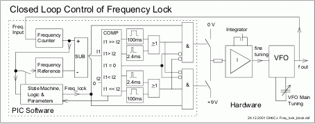
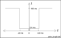
Figure 1.Block diagram of the frequency lock control. Frequency ReferenceFrequency reference is formed from the measured frequency itself after the delay defined by parameter 0Dh, when the number of the consecutive samples (defined by 0Eh) of measured frequency are within the +/-20 Hz. Then the actual value is trigged as frequency reference until the SW detects that the lock conditions are not valid. Frequency ActualFrequency actual is formed from the frequency counter function itself. Subtraction and ComparatorFrequency is measured every 100 ms. Next the frequency actual is subtracted from the reference and the difference is compared to value zero to calculate the deviation. If the result is zero, it means that no deviation and also no need to fine-tune the oscillator frequency. If the result is negative it means that the frequency actual is higher than reference. This detects the direction of the needed frequency correction. Next the rough value of the difference is calculated. If within 20 Hz then only short 2.4 ms pulse is controlled. If bigger then 100 ms pulse is controlled. By means of these few calculations we have information how to fine-tune the frequency of the oscillator to hold the frequency actual equal as frequency reference. Simple, is it?
Figure 2. Control pulse length as a function of the frequency deviation. Digital OutputsThese pulses are controlled to digital outputs RB0 or RB3 according to the sign of the frequency difference. The outputs are never simultaneously on because it means almost short circuit.
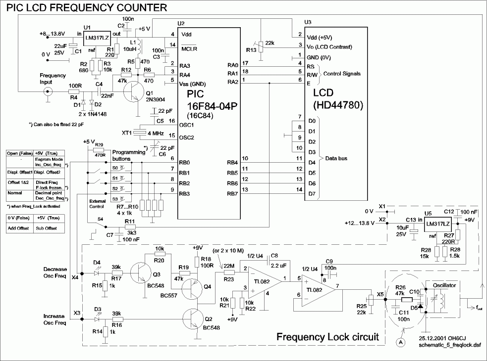
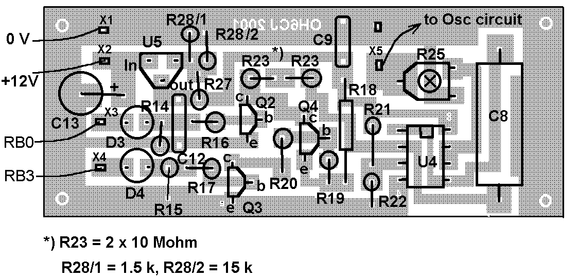
Figure 3. Schematic diagram of the frequency counter and frequency lock circuit. IntegratorThe controller is made using TL082 operation amplifier. The first amplifier is an integrator by means of the capacitor C8 and R23. A time constant is R23 * C8 = 22 M Ohms * 2.2 uF = 48 s. So the control is slow and it only fine tunes the oscillator frequency and this is of course the purpose of the controller. The VFO itself must be stable enough. Second amplifier of TL082 is connected as a buffer. Transistors Q2…Q4If the PIC SW controls the output RB0 to state TRUE, then led D4 is light and Q2 saturates. It connects integrator input via R23 to GND and the voltage at the output pin 1 changes to positive direction. If the RB3 is controlled to state TRUE, D4 is light and Q3 connects the base of the Q4 to ground. As a result Q4 is saturated and +9 V is connected to the R23. Now output changes to negative direction. If none of RBs are controlled, the integrator acts an analogue memory. It holds the last value at the output. This suites well for the situation where the subtraction result of reference and actual is zero. The used transistor types are not critical. Connection to OscillatorIt must be added a capacitance diode connection to the oscillator circuit. See area A in the schematic diagram. This additional connection changes the frequency range of the oscillator. So it must be compensated by tuning the frequency range of VFO, if necessary. Output of the buffer amplifier (pin 7) is connected to the trimmer potentiometer R25. This is used to scale the effect of pulse to the oscillator frequency. How to tune?
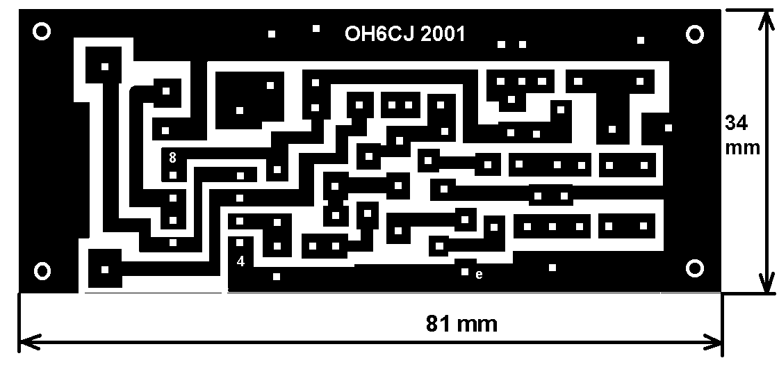
Figure 7. Printed board view from the bottom side PIC SW in the frequency counterDownload the LCD4DIEP.HEX file or source code. It is compatible with LCD4DIEC.HEX concerning the frequency counter functions. See the parameter setting instructions from the LCD4DIEC document. The configuration bits must be set: Oscillator = XT, Watchdog Timer = OFF, Power Up Timer = OFF, Code Protect = OFF Table 1. COUNTER MODE I/O functions when the freq_lock function is activated
ParametersTable 2. EEPROM-parameters 00h...0Fh functions
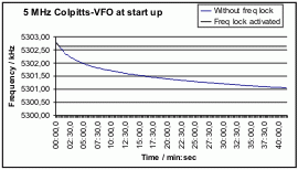
Final testIf the previous tests and settings have been successfully performed, it is a time to do connections between the frequency counter and frequency lock printed boards as well as connections to the oscillator circuit. Activate the Freq_Lock function by par. 0Bh. Reconnect the voltages to the boards and start to observe the LEDs D3 and D4. When the frequency reference has been sampled and set, the character “L” is displayed in the LCD. Observe the LEDs. Only short pulses should be seen seldom if there is a need to fine-tune the oscillator frequency. Long pulse can only been seen if the VFO drifts over 20 Hz within the 100 ms. A long pulse can be seen as a bright light (D3, D4) and short pulse as a dimmed one. The VFO that I have used in my transceiver, with the “warm” oscillator only few pulses can be seen during the 10-second period. At the beginning with “cold” VFO long pulses with short ones can also be seen. The effect of the control is too big, if correction to one direction causes immediate correction to other direction. Then reduce the effect by turning R25 a bit to counter clockwise. If a long pulse lasts several seconds before out of lock situation, effect is too small. Turn the R25 a bit to clockwise. It is good also to monitor the output voltage from the pin 7. The voltage should stay within the range of the amplifier output (about 0.5 V…7.5 V depending on the type of the used op. amplifier) so that minimum or maximum limit is never reached during the normal operation. Conditions to go out of Lock State are the consecutive number of samples (0Eh) which are outside of +/-100 Hz window. It is good to receive a stable carrier on the band and listen it when pulses are controlled. The audio frequency of the carrier must be remained stable. As well you can observe the stability of the 10 Hz decade in the LCD. I have now tested this few months in my 80 m SSB/CW transceiver. I had to add a buffer amplifier using JFET to isolate the RF effect to the frequency measurement circuit. Otherwise during the transmit RF caused disturbation to the measurement. RB2 FunctionA frequency lock function can be frozen with digital input RB2. How ever the last frequency reference is still set in the registers. This function can be used e.g. with direct conversion RX where TX offset is needed during the transmit period. A character “F” (Frozen) is displayed instead of “L” after the MHz text in the LCD display. Is this worth to build it?Above all this software is as is. No guarantee for any functions. However I am satisfied for this SW and electronics. I don’t need a separate switch in the front panel to lock or unlock the frequency. This SW with HW does it automatically. Remember that this circuit does not repair a bad VFO at all, but with a good one, it compensates the long term drifting and makes it even better to use. It is nice to listen to the certain frequency on the band without continuous frequency corrections after a little while by means of the VFO knob. | ||||||||||||||||||||||||||||||||||||||||||||||||||||||||||||||||||||||||||||||||||||||||||||