What DigiVFO is?
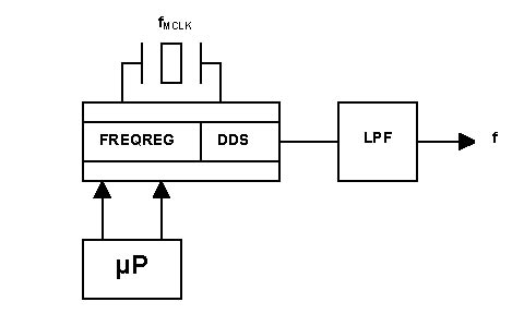
During designig of various receivers and transceivers I met a question how to make a simple, durable and economical oscillator, which would be reproduced with same quality. Because in my profesional life I am involved in design of electronic communication devices, I found, that an easy way will be with a DDS. From all possible I selected AD9834, which is small and consumes only 25mW. AD came latelly with a 75MHz version. Together with a good quality crystal oscillator and simple microprocessor could be build very nice tunable source of high quality signal from a couple of Hertz up to nearly 25MHz (up 32MHz for CRUZ version).
Who initiated it?
This article I wrote as a replay to a need of a simple, stable and economical VFO oscillator. From very beginning I concepted it only as an oscillator with DDS, but later I realised that the oscillator to be more useful must have some sort of control and posibility of setup and so a new project by name of DigiVFO has been born.
How is it designed?
....
How you can make it
The DigiVFO you can build on your own from documentation which is shown futher down or you can order from me fully assembled and tested PCB with all SMD components or PCBs only.
In the case you choose to do it on your own, it offers the HAM about 40hours to put it together and make it operational.
The DigiVFO supports three different type of tuning devices. Two push-buttons for UP and DOWN incrementation, as shown on the block diagram,
pdf
mechanical encoder with 24 pulses per revolution and electronic encoder with 100pulses up per revolution. The DigiVFO can be assembled with two diffrent X-tal oscillators; 50MHz or 67MHz. For other frequencies you are required to recalculate frequency table in EEPROM.asm.
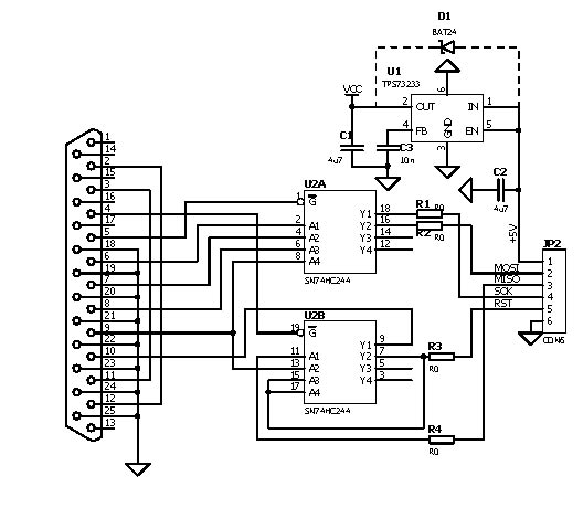
Schematics
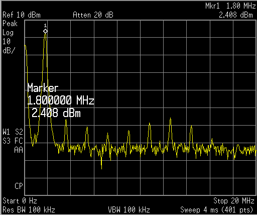
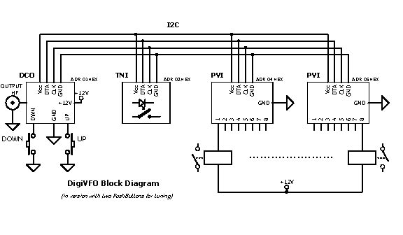
The DigiVFO project consists of a main block - DCO and several interfaces. In front of I must say, that DCO can be operational on its own and for tuning function does not necessary need any other interface. On power up it starts with parameters given in the eeprom.asm table as for channel 1. By default it is 1.8MHz.
The DCO can be driven by three different types of tuning devices. The simplest are two Push Buttons, one for UP, the other for DOWN. By pushing one the output frequency increases or decreses. In the file it is compiled to DigiVFO1.hex. Second one is a mechanical rotary encoder, like one you have on your microwave owen. The file for this option has a name DigiVFO2.hex. Last one is an electronic encoder with 100 changes per one revolution. File for it is in DigiVFO3.hex.
Next modules, connected over I2C communication port are TNI - control boards and and PVI output relay boards. When are used, they allow to build a communication device with frequency band switching. When powered, the channel one is connected, on DCO is turn on 1.8MHz oscillator and on TNI is switched on an indication LED for channel one. The PVI modul switches relay for channel one. In application does not matter if there will be relays or silicon, one can choose what will need.
Logically when other PB on TNI is pushed, turns the appropriate LED on and turns off the previous one. The PVI will react likewise.
The DigiVFO-DCO schematic in the pdf format is here. This shown version is ver. 1.3 - one of latests, but the development continues and suppose it still is going to be changed. Please take this as an informal drawing for now, which was tested, but expects, that a new functions and circuitry will be added.
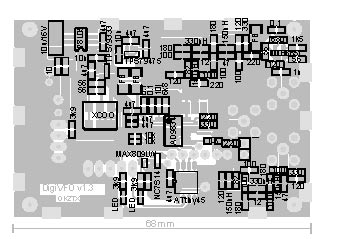
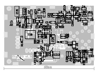
PCB for DigiVFO
For the DigiVFO PCB in the pdf format look here This print is from components side and is in 1:1 ratio.
The drawind of the PCB with SMD components.
and
pdf .
Futher you can see PCB with components name.
and
pdf .
On this picture you can see a prototype board of DigiVFO on the double sided PCB, just without plated holes. Final version has printed silkscreen mask.
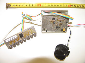
TNI MODULE
A simple module to control DCO is a TNI module. It consists of eight push-buttons and eight LEDs. By default the DCO after power up sets frequency which is tight to the first PB even the TNI modul is not conected. Frequency table is described by EEPROM.hex, before compilation in EEPROM.asm. You may do changes to select different frequencies and phase to each PB by changes in this file.
Every next push initiates a new frequency reload and confirmation by appropriate LED.
The module has only one IC. For communication over I2C it is PCF8574AT - remote 8-bit I/O expander for I2C-bus. By construction be careful, it must be an A version. In another case the module will not work because of different slave address. On the board exists posibility to setup four different addresses as shown on schematic diagram. Power for this module comes from DCO.
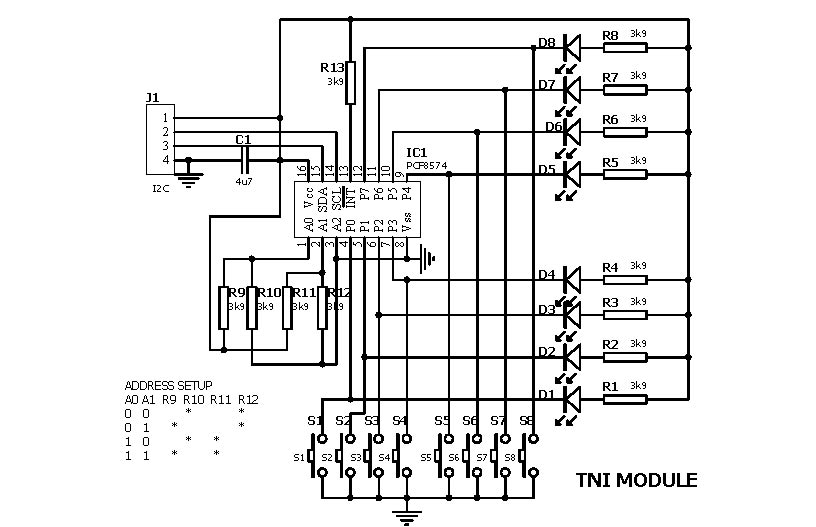
The TNI module is built on single clad PCB. Push buttons as well as LEDs can be assembled from both sides. Resistors R9 through R12 assemble as described in table on the schematic diagram. Only two of them will take place.
The artwork for TNI module is again in PDF format for immediate use. It takes you not too much over four hours of your time to build it.
Just look at the artwork and component side assembly .
Program and programing ...
You can use programms for DigiVFO I wrote, but you will need a programmer adapter for PC parallel port and a program to download it to the processor. The one which I use is gnu and its name is avreal. The adapter has a name STK200-300, an appropriate parameter to choose in avreal is -as. (Also you can use -az Lazy Blaster setup). I used recommended circuit and I only redesign it to make a documentation for an easy manufacture. The programmer looks like one on the following picture. It is placed into DB25 shell.

The schematic drawing is on next picture. The circuit is very simple, only what you have to care of is need for right wire connection. Just check up if they are correctly joined and measure all signals from HC244 to its position in DigiVFO.
and for better view
in pdf .
I am also using this adaptor for programming other AVR processors, so on the PCB are some provisions, which you may not use. The voltage regulator U1 is employed only with processors supplied with 3.3V. In other cases is assembled a diode D1 instead and place for regulator is left empty.
If you decide you will make it, download a PCB layer in pdf format in 1:1 scale for direct print. The picture is in left bottom corner.
Batch file for program compilation c.bat
Batch file for EEPROM compilation ce.bat
Compiled program is in a downloadable format eeprom.hex and digivfo.hex
Complete download of all programs and data for loading it in to the chip digivfo.rar
Measurements
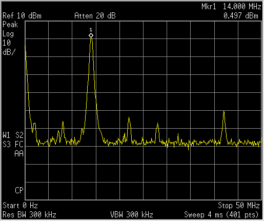
The DigiVFO put together generates harmonic output signal. Following pictures are taken from very basic unit with ordinary 50MHz XCO, inductances in LPF with Q less than 10.
On each of push-button push it starts to generate different frequency. In my case from 100kHz up to 21MHz. The whole range is much larger, the DigiVFO can be tuned from couple of Hertz up to 24MHz. Especially higher bands must be used with consideration of what it will be used for. The signal becomes very dirty as goes close to 25MHz. (it is half of X-tal oscillator frequency).
Limitation of this unit built is low inductance quality used in LPF on the DDS output, which presents on measument peaks of 2nd harmonics (3rd as well). The LPF characteristic is not flat enough, thus amplitude of 100kHz signal is much larger than amplitude 14MHz one(-8dB).
On the trace of 100kHz are seen some clippings, signal is squeezed due to low attenuation and high voltage input into output OpAmp. It is corrected by a resistor divider in ver. 1.4.
On CRO pictures red trace is calculated FFT and blue trace is actual output signal. The FFT does not generate good enough results as a spectrum analyser so it should be taken as an informative graph, thanks the method of calculation.

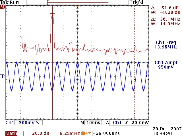
And finaly on last pictures you can see measured signal spectrum on the DDS output, after being amplified.
...............................................................
|