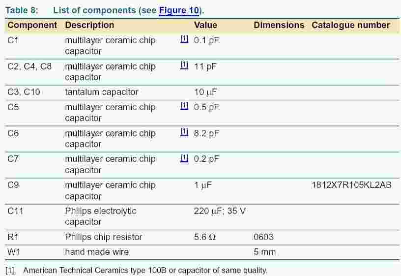
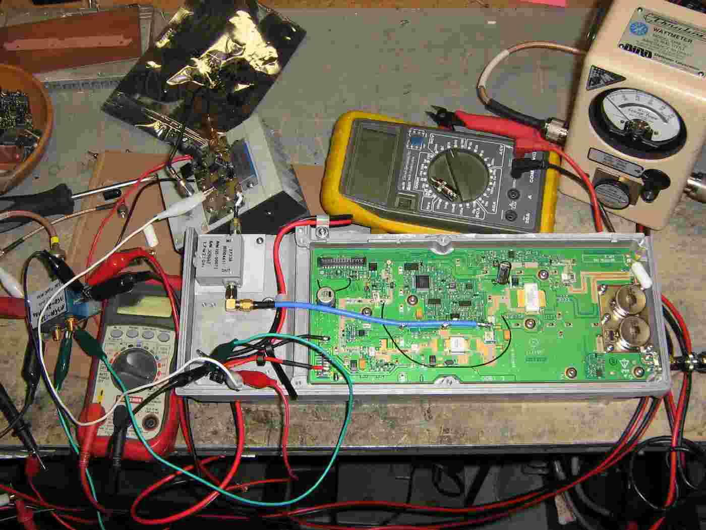
Stock RF power amplifier section of a 1.9 GHz cellular phone base station module. FCC ID: L7KTSPB-01.
The RF input circuitry is on the left-side, RF output is on the right. The silver circular part is the output RF isolator.
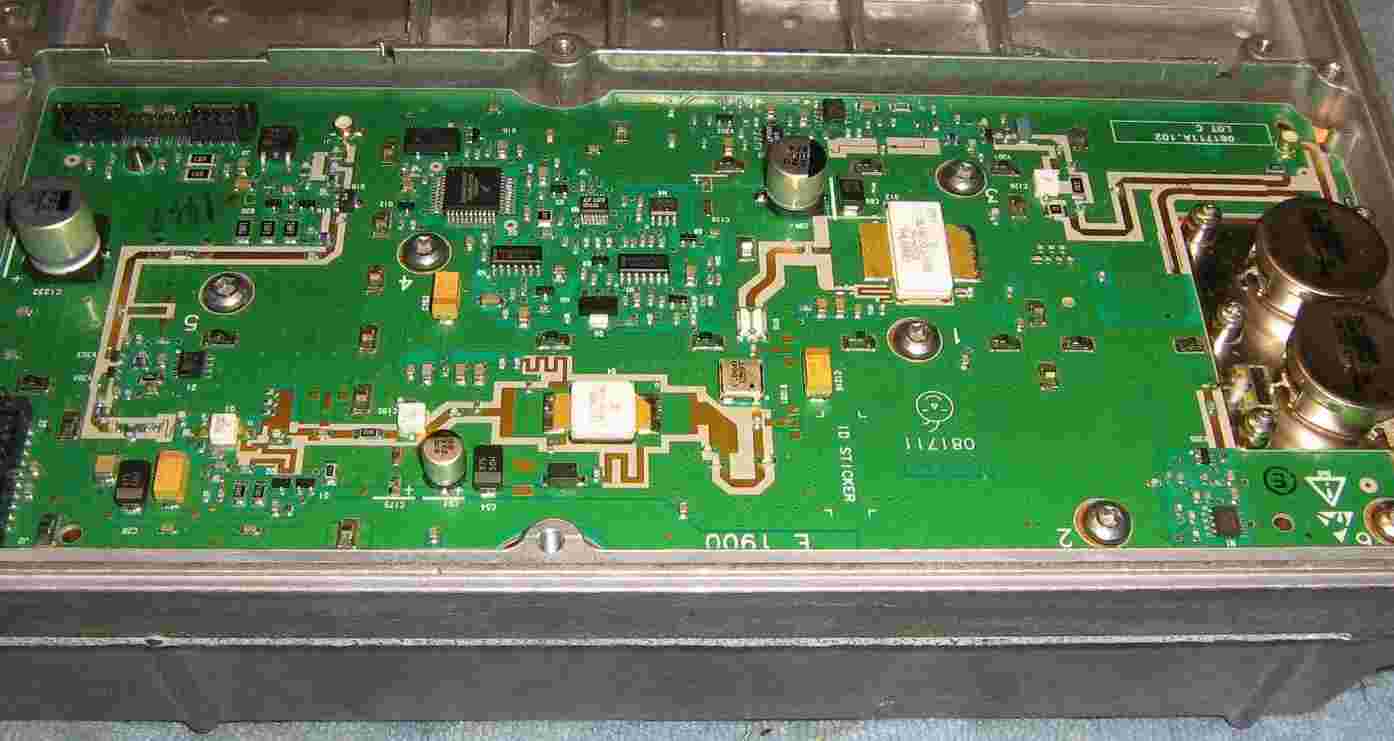
Close up of the RF input circuitry.
The smaller white transistor on the left is a MRF281Z, which feeds a MRF19030LS.
We won't be using the pre-amplifier transistors in this amplifier, but they may be documented in an upcoming project.
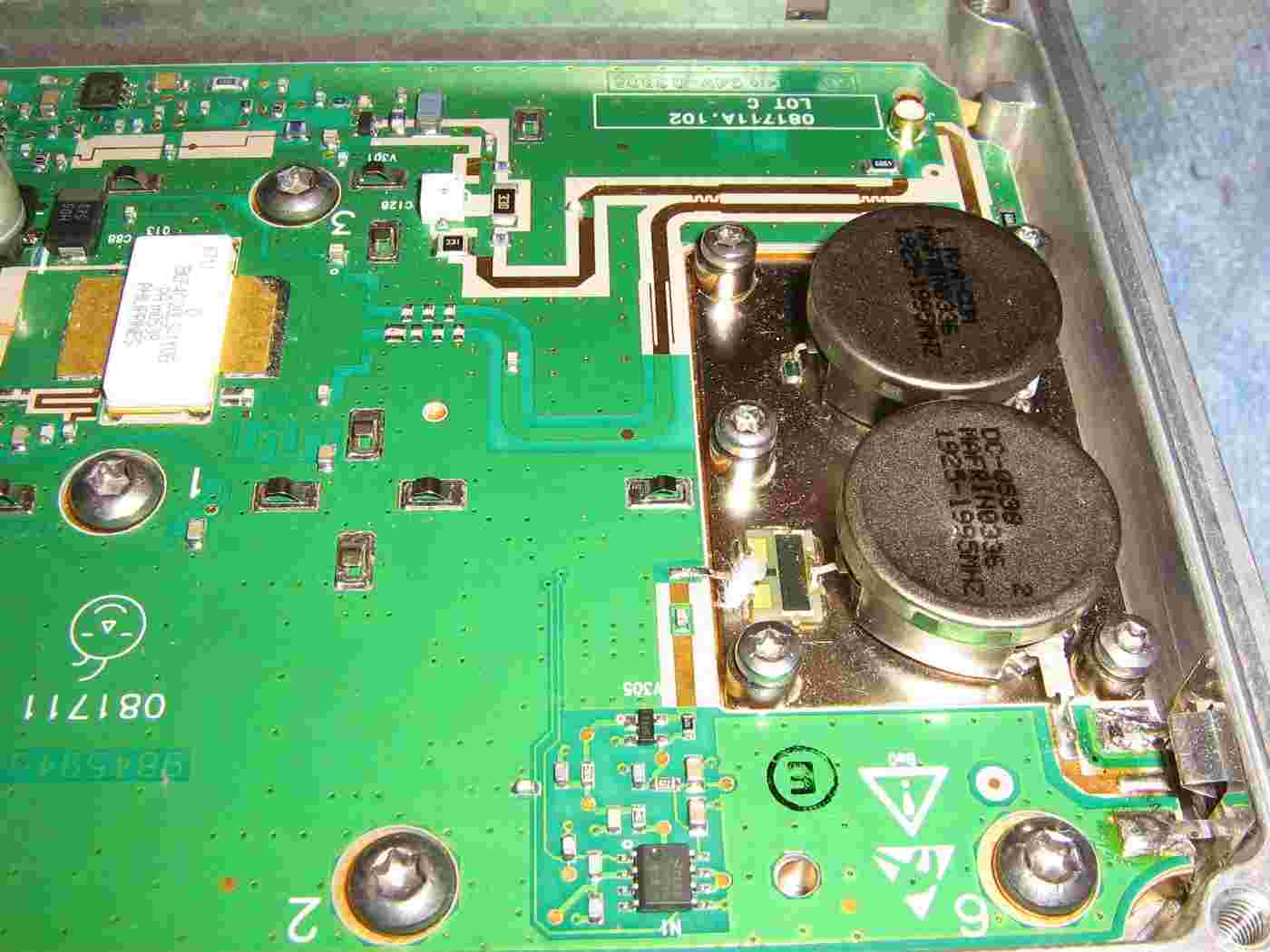
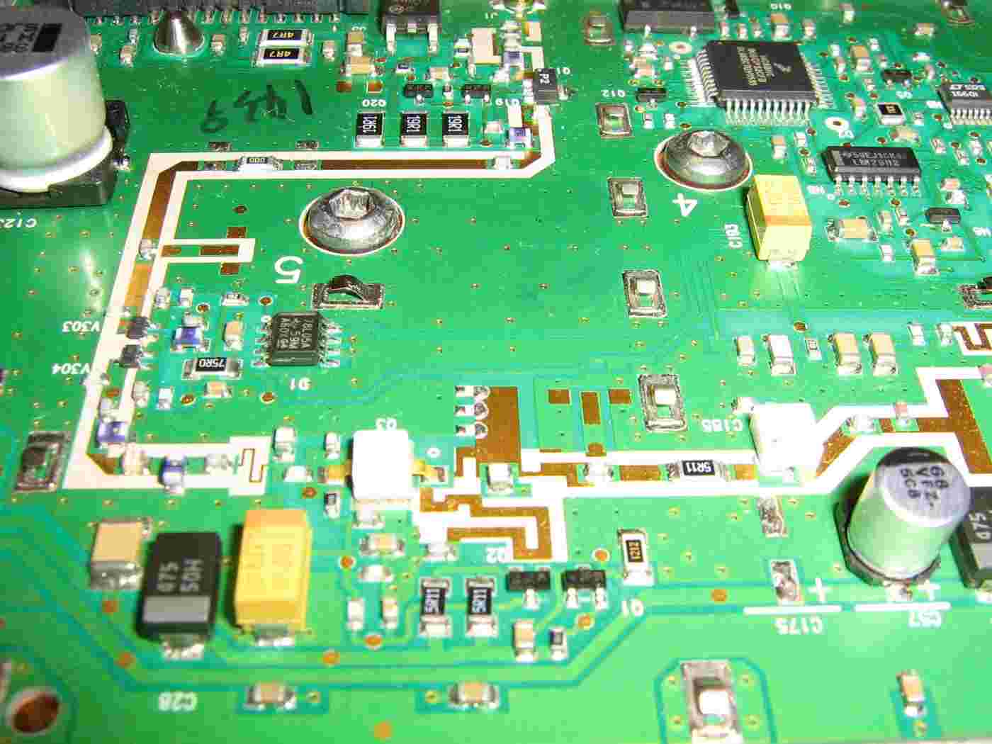
Close up of the RF output circuitry and isolator.
The SMA RF output connector is on the lower-right.
The top PC board traces form a directional coupler to monitor the BLF4G20LS-110B's RF output.
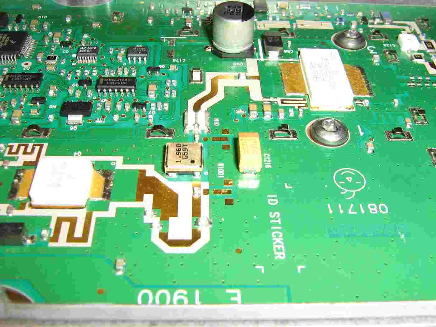
Input circuitry and impedance matching section for the Philips BLF4G20LS-110B. The MRF19030LS is on the lower-left. The silver box in the middle is a 1.96 GHz bandpass filter.
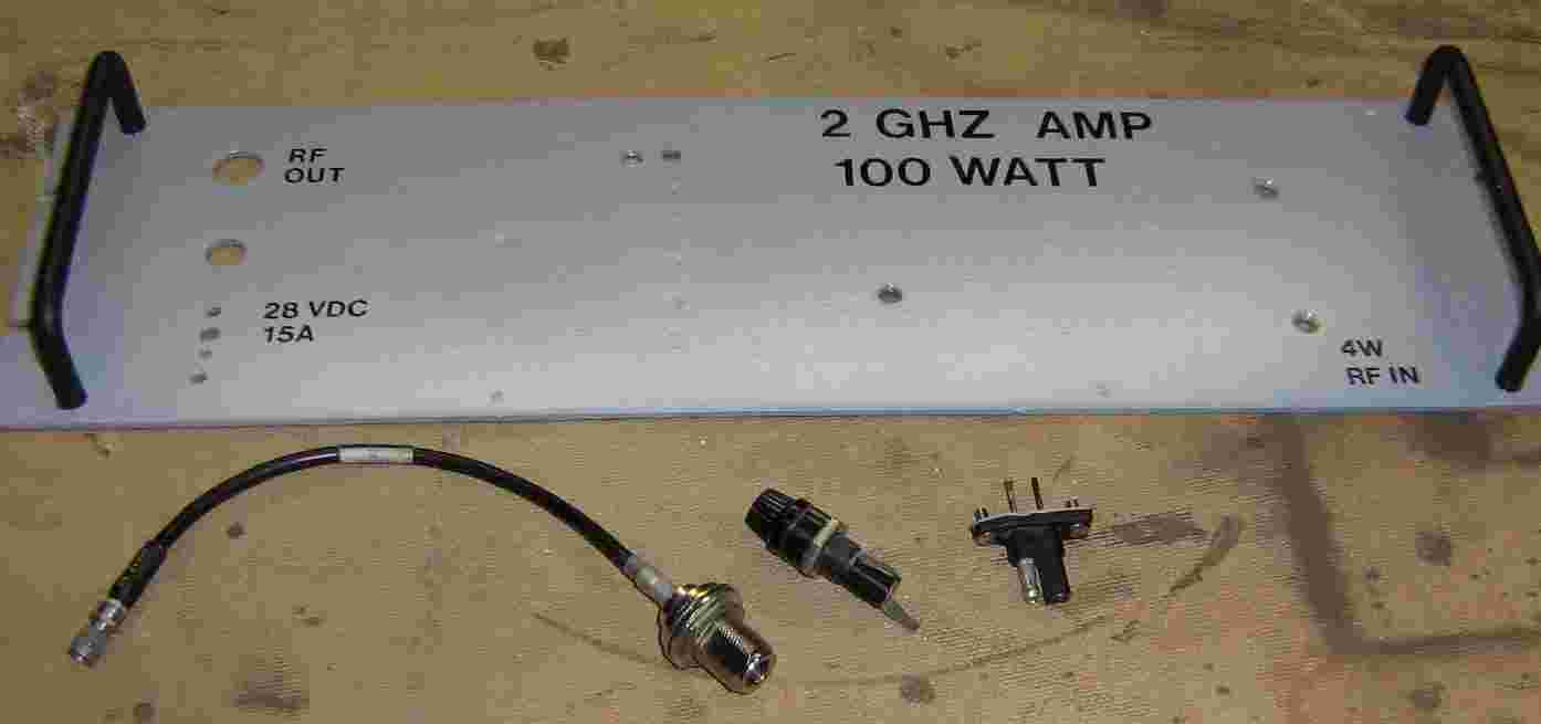
The front-panel to the rack-mounting system we'll be using for this amplifier.
The panel was salvaged from an old rack-mounted power supply and some of the holes were filled with Bondo. A fresh coat of paint, labels, and clear coat help to finish it off.
The RF output will be via a panel-mounted female N connector.
The +28 VDC input will be protected with a 15 amp fuse.
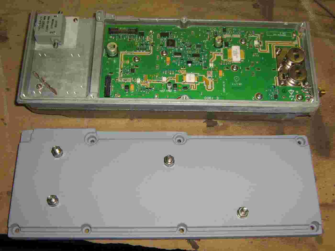
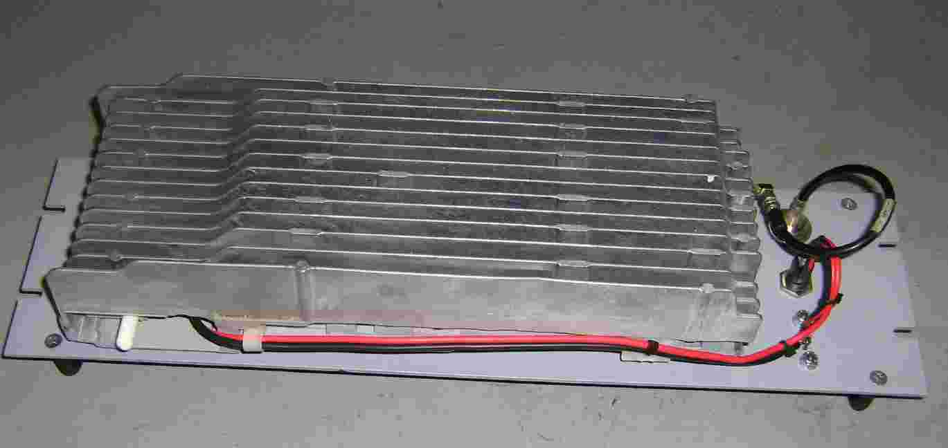
Modifying and cutting down the module's original aluminum case so it can be mounted to the front-panel.
The amplifier case will be attached to the front-panel with four 1/4-inch bolts and hardware protruding through its cover.
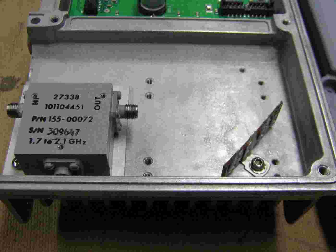
A salvaged 1.9 GHz-band isolator was added to the input of BLF4G20LS-110B. This is to help solve any stability problems, but may restrict the amplifier's overall frequency range. This input isolator is optional.
A solder terminal strip was added on the lower-right for centralizing the DC input power connections.
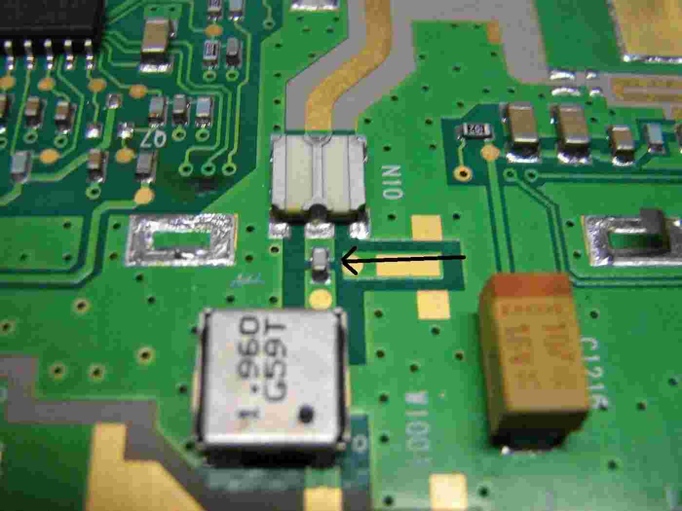
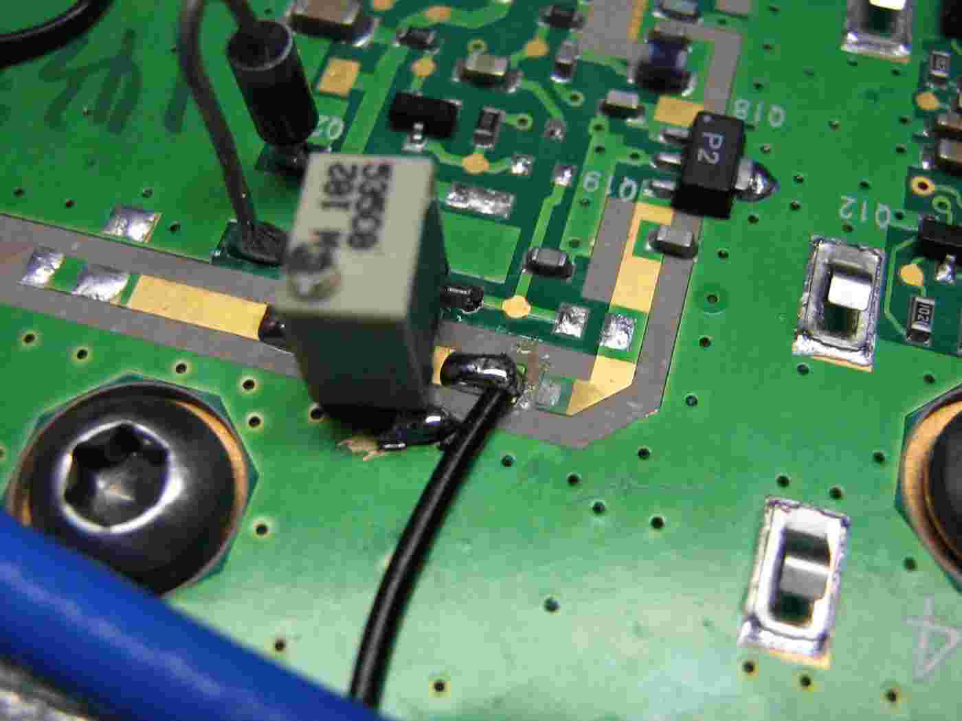
Arrow points to a series capacitor which will need to be removed to isolate the input to the BLF4G20LS-110B.
This is first of several modifications which will need to be done in order to use the amplifier.
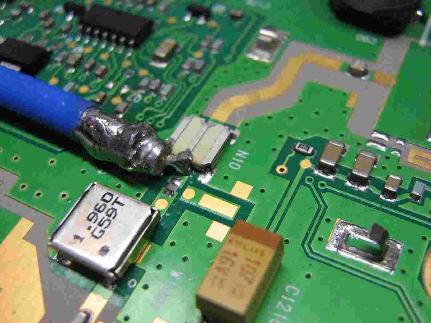
After that capacitor is removed, solder a piece of 50 ohm coax for the RF input to the BLF4G20LS-110B.
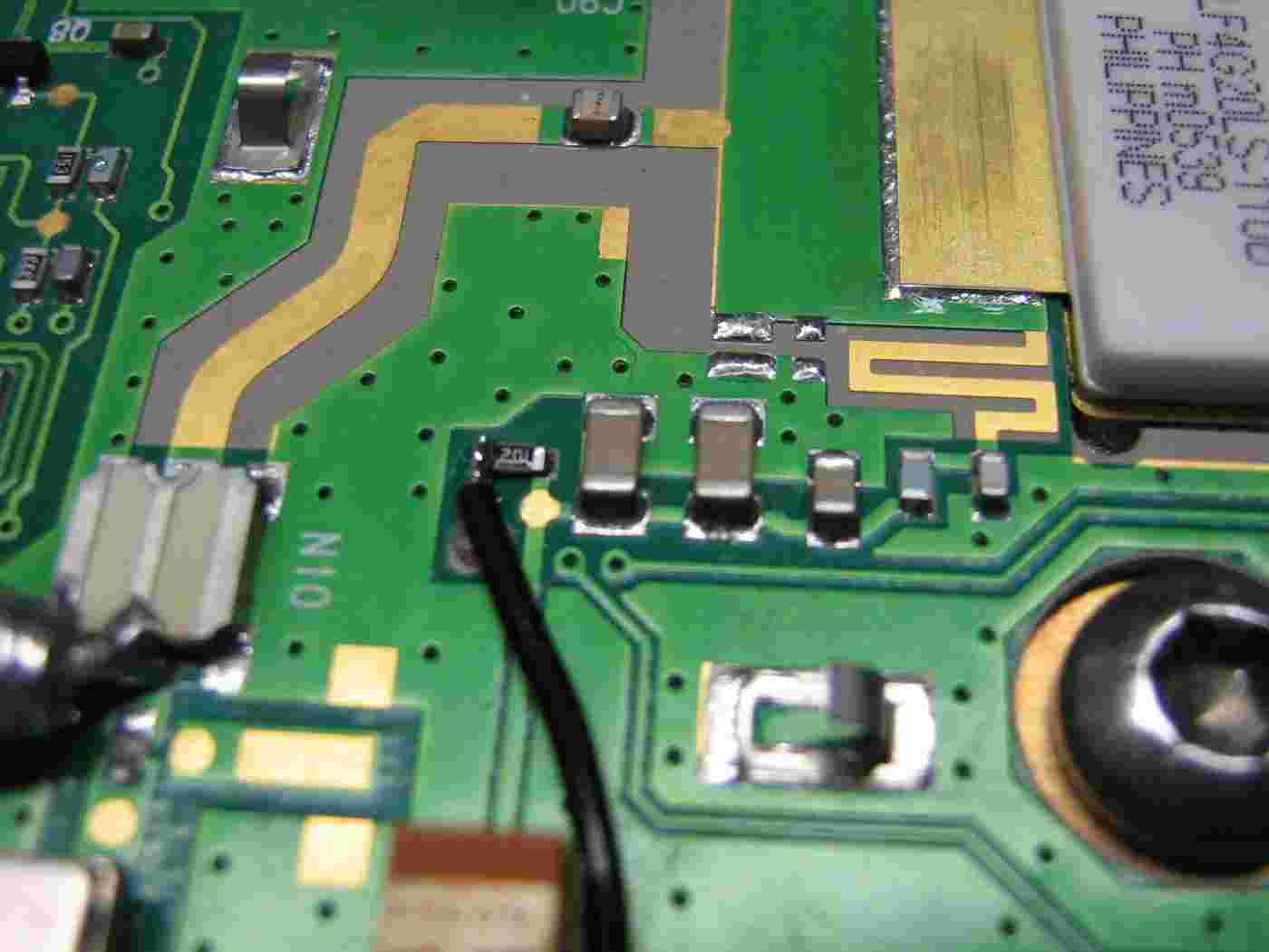
Solder the center of the coax to the surface-mount jumper device labeled "N10" on the PC board. Scrape away some of the amplifier PC board's top coating and solder the shield of the coax to the ground plane.
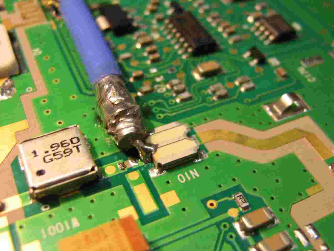
Alternate view.
Try to use Teflon dielectric coax to avoid any melting and to ease soldering.

+28 VDC power input connections.
The BLACK wire is NEGATIVE.
The RED wire is POSITIVE.
Unsolder the amplifier's original power input terminal strip and solder the power connection wires like so. The negative wire is actually going to an unused solder pad on the amplifier's ground plane.
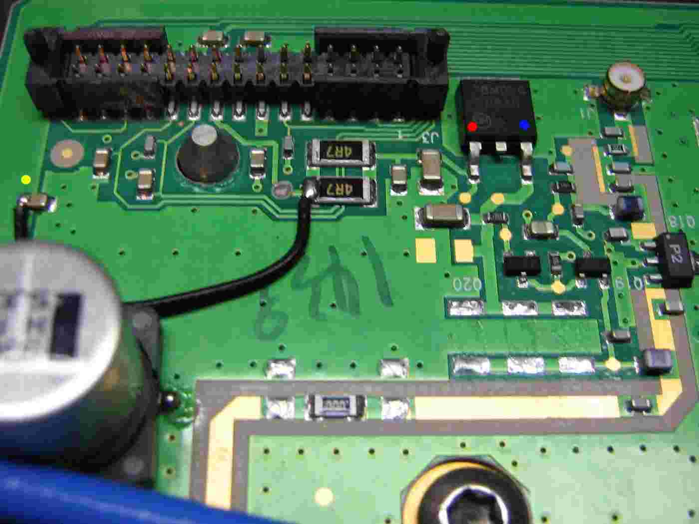
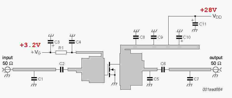
The BLF4G20LS-110B requires an approximate 3.2 VDC bias voltage on its gate for proper class-AB operation.
To generate this voltage, we'll isolate and use a 78M05 voltage regulator on the amplifier circuit board.
In the above picture, the YELLOW dot is the +28 VDC input for the 78M05. The RED dot is the input pin for the 78M05 and the BLUE dot is the 78M05's output.
Note that you'll need to follow the traces on the output of the 78M05 and remove three series resistors, as shown above.
Solder a jumper wire from the YELLOW dot (+28 VDC) to the two parallel 4.7 ohm resistors on the input of the 78M05.
After removing several unnecessary components on the output of the 78M05 voltage regulator to isolate the solder pads, you'll need to add a series 1N4001 diode and a surface-mount multiturn 1 kohm potentiometer. The series diode is optional, but helps to protect the BLF4G20LS-110B from exceeding its maximum gate voltage.
One side of the 1 kohm potentiometer will go the the +5 VDC and the other to ground. The wiper output will go to the gate bias circuitry near the BLF4G20LS-110B.

BLF4G20LS-110B gate bias components.
You'll need to cut the trace were the arrow is pointing to isolate it from that feed-through via.
We'll be isolating this bias line and adding our own gate bias voltage.
Solder a wire from the wiper of the 1 kohm potentiometer on the output of the 78M05 to the 1 kohm resistor in the BLF4G20LS-110B gate bias input, as shown above.

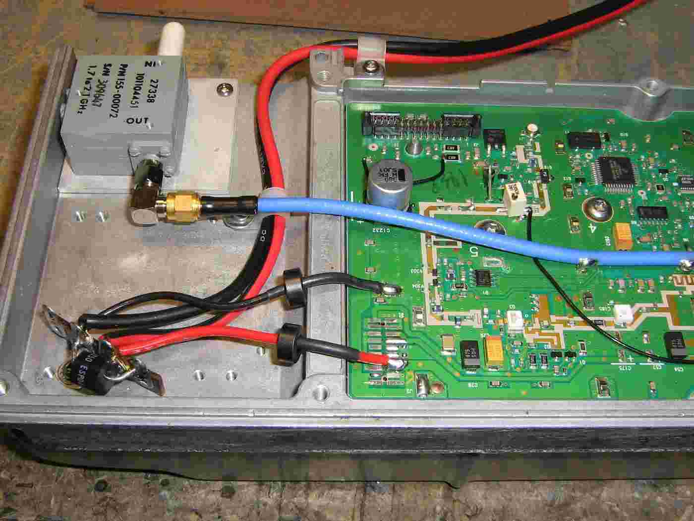
Overview of the modifications performed so far.
Finishing and connecting the DC power input connections and RF input.
Optional ferrite beads were slipped over the DC power wires.
There is also an optional DC polarity protection diode on the solder terminal strip.
Setting the quiescent drain current on the BLF4G20LS-110B.
Connect good 50 ohm loads to the input and output of the amplifier and apply a clean source of +28 VDC power through an accurate current meter.
Slowly adjust the 1k ohm gate bias potentiometer until the amplifier is drawing around 650 mA of current with NO RF power applied. This should be equal to around 3.2 volts DC on the BLF4G20LS-110B's gate.
Let everything "warm up" for a bit and see if the quiescent drain current varies at all over time. It should be fairly stable when set.

Rear view of the front-panel showing the DC input wiring and fuse, and the panel-mounted N connector for the RF output.
Rear view of the amplifier showing the DC power and RF connections.
The white cap protects the SMA connector on the input RF isolator.
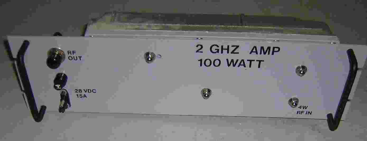
Finished amplifier front-panel overview.
5 watts in gives around 100 watts output at 2 GHz. I'll keep fiddling with it to try and get more RF power out at 2.3-2.4 GHz.