Printed Circuit Boards Using Toner Transfer
Ā
Producing the artwork
Toner Transfer is a fairly easy way to make printed circuit boards. Artwork can be copied from existing art work from magazines, or created using CAD programs. I have used the freeware Lite version of EAGLE CAD (now known as Autodesk EAGLE) starting from version 4.16 and the board image produced by ExpressPCB (exported as PDF), or a graphics program such as MS Paint can be used. For Linux (or Windows) The Gimp, an open source program is available. The one that I like best is PaintDotNet, freeware originally developed by Washington State University and Microsoft. A big advantage is the way it handles layers, and repetitive cut and paste. It is especially useful in retouching the art work produced by the CAD program.
I typically develop a board design using EAGLE, and either print it directly or export it as a .bmp file for editing in a graphics program. By doing that, I can add text, thicken lines when needed, and often I'll do some selective fill in ground plane areas. It is certainly not necessary to do this, but I just like to do a bit of final editing. One tip: convert the .bmp image to .png early in the process; the .bmp image file size is very large. KiCAD is another favorite CAD program among the amateur radio community, especially those who want to export gerber files to be sent to PCB houses for production.
Selecting the transfer media
When I first started making PC boards using the toner transfer method (ironing an image onto a PC board, as opposed to using presensitized boards and photographic methods), I used a commercial product, Press 'n Peel Blue. I've also used an alternative media (paper), which is free. More on that later. The artwork is used as a reversed image and either printed directly on Press 'n Peel Blue (by Techniks) toner transfer sheets using a 300 DPI laser printer, or printed on paper using an inkjet and then photocopied onto the material. Laser and copier toner is plastic based. Press 'n Peel Blue is available from Techniks.com, tindie.com as well a several other vendors. 20 sheets of Press 'n Peel Blue are $33 on the Techniks website in December 2023. Electronix Express (www.elexp.com) sells a 5 sheet Hobby Pack for about $10 (as of December 2023).
If you visit the Techniks website, they have a note that reports from users indicate that the product does not work well later model Brother copiers and laser printers. I contacted them about that several years ago, and their tech support said Brother machines use higher temperature "ink" (actually, plastic particles) than other laser printers. I had a Brother printer at that time. I've used an HP 3050A laser printer since 2017.
A disadvantage of Press 'n Peel blue is that it is relatively expensive. What I have been using since 2017 is yellow thermal transfer paper from sources in China. A search on "toner transfer paper" will return several sources for that paper. Amazon has 20 A4 size sheets for $8.99. I have found that it produces very good images. The image is created on the shiny side, unlike Press 'n Peel Blue.
Preparing the board
The bare copper circuit board surface must be clean and free of surface defects or staining. It should be scrubbed with steel wool, very fine sandpaper, or "greenies". The final step is to chemically clean the board with acetone. After that, the board surface should not be touched with bare fingers. Alcohol of any type is not a substitute for acetone.
Getting the image onto the PCB
One thing I've found out through experience is that the steam holes in a typical iron tend to initially produce some wrinkling, especially around the edges of the board. A good solution would be to find an old-fashioned steamless iron at a GoodWill store. I have a small steamless iron that I've used. When using a steam iron (without the steam!), the iron has to be kept moving.
An advantage of Press 'n Peel Blue and the yellow toner transfer paper over some alternative media to be discussed later is that it deposits a hard layer of plastic over the toner image on the board, acting as additional resist and generally producing sharp lines. Whichever media is used containing the image, it is then ironed onto a cleaned and prepped (steel wool or abrasive pads) blank printed circuit board.
With the toner transfer process, it is fairly common to produce boards with small patches where the material did not adhere, probably due to the board not being properly prepped in those areas, or localized uneven heat transfer while ironing. These areas can easily be touched up by going over them with a permanent marking pen, such as a Sharpie, or with lacquer-based fingernail polish. In the first photo, you can see areas where I've applied a contrasting color of fingernail polish to a couple of the boards. While making the board for a 40 meter transmitter recently, even after applying fingernail polish to a couple of areas where the blue material didn't stick, the polish came off during the etching process, indicating that the chief culprit of gaps is inadequate preparation of the blank PC board stock.
Etching the board
After the boards have been etched in ferric chloride or other circuit board etchant, the Press 'n Peel Blue has to be removed from the copper foil. During this step, it becomes evident just how tightly bonded the plastic from the toner and Press and Peel Blue have become to the copper. Prepare for a few minutes of strenuous exercise with a Scotchbrite ("greenie") pad. Using some acetone will hasten the process tremendously. Hint: try it first without the acetone, and you will discover just how tough the Press 'n Peel layer over the copper traces is. Ferric chloride is available at Micro Center, possibly at some of the remaining Radio Shack stores, Amazon, eBay, and jameco.com.
An alternative to ferric chloride is hydrochloric acid mixed with hydrogen peroxide. The chemical reaction produces fumes that are dangerous. It does etch the board faster, and some swear by it. I have not used this method. If you want to try it, it is important to get explicit instructions on the process, particularly mixing the two chemicals.
Examples
Some boards done using Press 'n Peel Blue are shown below.
Click on the photos for a higher
resolution image.
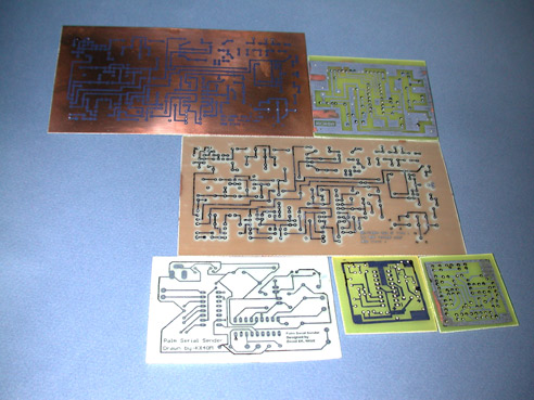
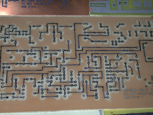
Several project boards
The board in the center of the group is the Belthorn SSB IF Module. You can see lighter areas around the pads; this is a double-sided board, the first one that I've done. The top side of the board is a ground plane, with etched circular areas around the component leads. Above and to the left is an un-etched version of the same board.
Closeup of the Belthorn board
If you look closely, you can see that the blue material is still on the printed circuit traces. It looks like the board traces are irregular, but they're not. I traced over the Press 'n Peel Blue material with a fine line permanent marker in most of the areas, which was probably not necessary. The irregular appearance is due to the contrast between the darker marked lines and the underlying blue material. After etching, the dark blue material fades to a lighter color, which can be seen in this photo and the first one. To avoid tarnishing of the copper traces prior to soldering the components on the board, I leave the Press 'n Peel Blue material on the board until ready for tin plating (optional; more below). Then, I remove the Press 'n Peel with acetone and the Scotchbrite pad. Plating the copper preserves it and improves solderability.
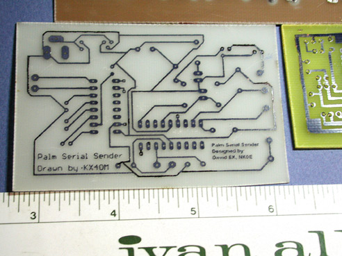
Palm Serial Sender
This board is one I made using Eagle from an article and schematic by David Eck, NK0E. It is an interface between a common Palm PDA and a transceiver, such as my SW20+, that provides contest logging and transmitter keying features from the PDA. Mine is a Palm IIIXE, although I have one of the original Palm Pilots that I might dedicate to this use. The board is a good example of the fairly fine lines that can be produced using the Press and Peel Blue process. There is only one very small section that I'll have to bridge, in the upper right corner in this photograph, when I solder the components to the board.
Preserving the copper traces
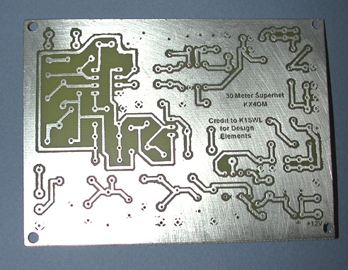
Example of a Tin-plated Board
This board has been tin-plated using the Tinnit product, which is basically a stove-top method. You clean the board to remove any lacquer or other contaminants, and put it in the solution for a few minutes at 130 to 140 degrees F. An alternative is Liquid Tin, a room temperature product that works extremely fast. I prefer it over Tinnit, although the tin layer appears to be thicker with Tinnit. The board is for a 30 meter superhet receiver based in part on at least three of Dave Benson, K1SWL's designs (note the credit etched into the board). I built the design, and it is shown in my Projects section of my website.
Alternatives to Press 'n Peel Blue and yellow transfer paper
Early on, I consulted with the Homebrew_PCBs Yahoo group to find alternative media and/or methods that would be (mostly) free. NOTE: The Yahoo Group Homebrew_PCBs has been transitioned to the groups.io group groups.io/g/homebrewpcbs. After trying several types of paper, including plain clay-coated inkjet paper, glossy inkjet paper, and several other types, I achieved my best results using paper cut from the mailed 8" x 10" version of the Harbor Freight tools catalog. Others have reported good results with Time magazine, etc, but the Harbor Freight catalog seems to have just the right amount of semi-gloss surface texture on the paper for my printer. Following are scans of some boards I've done (July/August 2006) using the new and very inexpensive method:
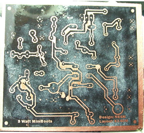
The image above (shot with a digital camera while the board was still wet) is an RF amplifier based on a design by Wayne McFee, NB6M. It was the first board I made using the catalog paper. There are a couple of defect areas that needed retouching. You will notice the white fuzziness over the black ground plane areas...this is residual fibers from the paper (one disadvantage over the plastic media of Press 'n Peel Blue). It is not necessary to remove all of this fuzzy stuff; only in the copper areas that will be etched away.
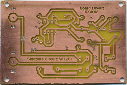
This board is a good clean board, the first one that I was really pleased with using the new method. You can see a few places where I had to rout out the traces, due to extraneous resist material still on the board while etching. I'll have to repair one of the traces. That notwithstanding, it is an acceptable board. It is a sidetone oscillator from EMRFD Chapter 1, combined with a relay to do some switching of the audio.
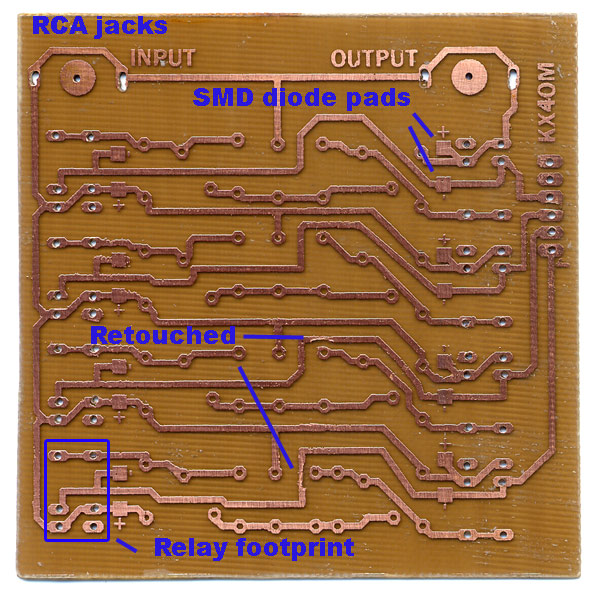
This board is a 4-band low pass filter board, switched by eight relays. It is to be used in a linear amplifier based on the WA2EBY design that was in QST awhile back, and I used relays instead or the rotary switch. The filters for 80, 40, and 20 meters are borrowed from the CDG2000 transceiver design, and I synthesized a similar filter for 30 meters using the RFSIM99 freeware program.
It is a two-sided board, this being the bottom layer. With EAGLE, it is possible to flip a surface mount component to the bottom layer using the "mirror" icon. I used surface mount diodes across the eight relay coils to save some space; the pads are indicated by the annotation. Notice that the "+" and"-" legends I added in Photoshop to the image are clearly visible in copper. There are two areas where I made corrections after ironing the image, and these may need to be beefed up by adding a component lead shunt soldered along the tracks. I drew the top side traces by hand (not shown), as they consist only of the RF paths from the RCA jacks to one pad on each relay. One thing to keep in mind when etching a two-sided board is to mask the side not currently being etched. When I was etching the amplifier board, I suddenly remembered that point about 3 minutes into the etch!
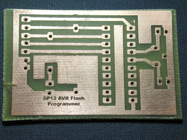
AVR Flash Programmer; board designed by Steven Bolt. Transfer using catalog paper. This board was made in January 2007. The resolution, as can be seen by the printing, is very good. The board is a simple AVR flash programmer that interfaces to the PC via the parallel port. I built it to program the AT90S2313 AVR for the ELSIE LCF meter with Morse code output. I made the photo with my Nikon N-990, without flash rather than scanning it, and the slight image distortion from the lens is evident.
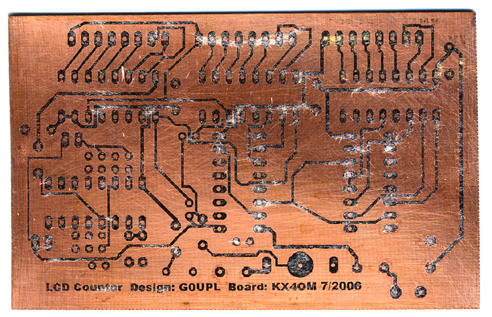
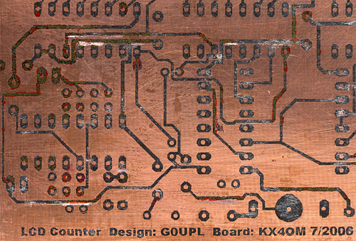
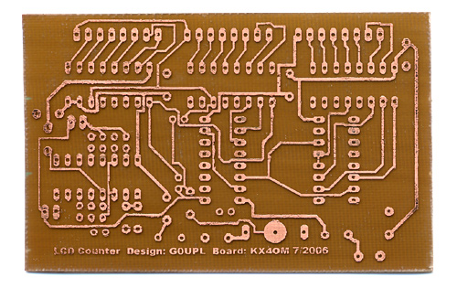
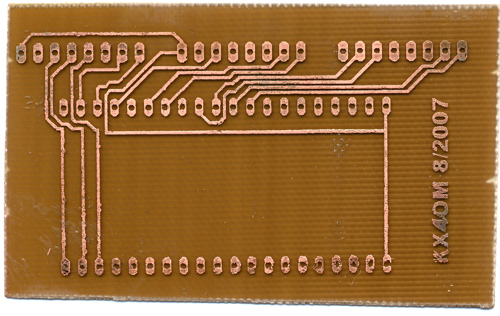
These two boards (not the same scale) are based on Hans, G0UPL's LCD frequency counter, to be used with a VFO I am building. The counter, unlike most designs currently in use, does not use a microcontroller, only logic ICs and and 7-segment LCD display driver ICs. The counter will display either a 3-digit reading kHz reading or, switch selectable, 2 digits with decimal, giving 100 Hz resolution. The readout will be kHz from the bottom edge of the band. I CADded the counter board based on Hans' schematic, and I did the display board based on the Luminex display's data sheet. The total cost of parts for the counter, including the display, is just under $10. These boards are to be two-sided; first I will have to etch the side shown in the image, then drill registration alignment holes in a few key pads used by both the top and bottom layers. When aligning the top sides for toner transfer ironing, I will hold the board up to a strong light, and fix the position of the catalog paper image over the alignment holes. When light is shining through all of the holes, I will then place the board down and immediately iron the image. It is a bit tricky, so obviously I try to design single-sided boards whenever practical.
For the first board, I photographed it with some paper fibers still attached in areas of the copper traces. If theses are not carefully rubbed off (a wet finger works well), the individual fibers are likely to interfere with the etching process. The result will be wisps of copper in the areas between traces, possibly creating shorts between circuits. Always do a high-magnification final check of the board prior to etching. I use an inexpensive head-mounted flip-down magnifier, and sometimes even scan the board at 300 DPI and compare it to the artwork. The fibers are one disadvantage of paper-based media; another is that the traces (black plastic-carbon toner mix) are not as durable as those produced by Press N Peel Blue, with its plastic top layer deposited on top of the toner.
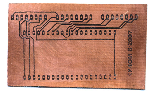
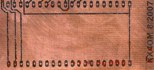
The second of the two boards is the display board; it shows the degree of fineness possible with toner transfer. The pads on the board are spaced .1 inch apart, and you can see that at the top of the board, I have up to six parallel traces of .014" width. This was my first experiment with such small traces and close spacing. The other board I've left for illustration partially cleaned. After an image is transferred, the board is soaked in water. After awhile, the paper is soggy enough so that it can be carefully rolled off the board in sheets. This process is repeated until all of the paper stuck to bare copper is rubbed off. If rubbed too aggressively, the traces will also gradually rub away. This can be seen for examining the bottom row of pads on the display board. Those will have to be touched up by pen.
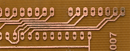
Above are closeups of sections of the two boards after retouching. Typically, this involves finding voids in the toner and filling it in using a permanent marker pen. If the pen colors too far outside the lines, so to speak, the excess marking can be simply scraped away. You may be able to see some scrape marks in the copper where I've done this. While prepping these these boards, I couldn't find my exacto knife, so I used the point of the smallest screwdriver in one of those ubiquitous 5-packs. As I mentioned before, I have one of those inexpensive head-mounted magnifiers, and I use that to get in really close. Also, the toner transfer process may have merged some pads with tracks where it was not intended. Referring to the original artwork can clear up any ambiguities. You can also see that the pad holes are not necessarily perfectly round after retouching. These holes simply serve as a Dremel tool drill bit positioning point. By the way, I have an older Dremel tool mounted in an older model Dremel drill press. I put a softwood block on the drill table, and the PC board on top of that, and drill by raising and lowering the table with its rack-and-pinion knob. The newer model Dremel drill press rig moves the tool up and down. For holes that have been filled in by copper after etching, I use a $2.25 spring-loaded punch I got from Harbor Freight on sale to make a good impression for the bit point.
Here are the two boards after etching. No surprises; however, I'll typically take a close look at them under magnification, and I'll flow solder on any tracks that are not very solid. An alternative is to apply self-stick copper circuit repair tape (soldering the ends), which is available in 1/16" and 1/8" widths from eBay or online vendors. Or, simply solder some appropriately sized solid copper wire over the defect.
The above image was scanned at 600 DPI to see how the critical .014" paralled traces look after etching. There don't appear to be any shorts between the traces, but I'll check them with a DVM prior to assembly of the display board.
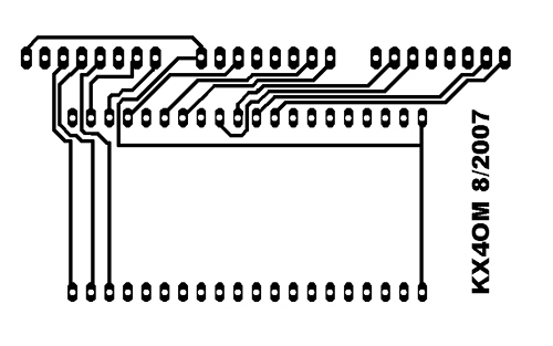
For comparison of the above pictures of the display board, here is the original art, flipped horizontally for normal reading.
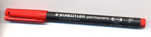
The final picture is the pen I usually use for fine retouching. The Staedtler Lumocolor Red was recommended by members of the homebrew_pcbs Yahoo group. They have a hard fiber tip. Sharpie marker pens can be used, especially for large areas. Unlike Sharpie pens, the Staedtler Lumocolor pens do not dry out nearly as fast. They can be left uncapped for several days without drying out (it says so on the label). I have had several last for over two years. Art stores carry the pens.