BEE
Semi Conductors
Basic Semiconductor Devices
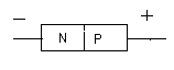
Modern semiconductor devices are made from selenium, silicon, germanium or gallium arsenide.
Impurities are added that increase the conductivity of positive or negative voltage potentials resulting
in materials that we call N-type or P-type. The adding of these impurities is called "doping".
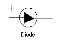
A semiconductor diode is a PN junction. When a positive voltage is applied to the + or anode terminal
and a negative voltage is applied to the - or cathode terminal the diode is said to be forward biased and
current will flow. The physical size of the device determines how much current can flow before it is
destroyed by heat. This determines the "I" rating of the diode. Depending on the type of material that the
diode is made of, the junction will have a voltage drop of either 0.3 or 0.7 volts.
If the voltages are reversed the diode is said to be reversed biased and little or no current will flow. The
limiting factor being the amount of voltage needed to break down the PN junction, shorting the device,
and causing permanent damage.
This is known as the PIV (peak inverse voltage) or PRV (peak reverse voltage).
Below is the schematic symbol.
In quick summary a diode is a one way valve for electric current. Whether it passes the positive or negative
portion of the applied voltage is determined by how it is installed in the circuit. They are often used in power
supplies to convert the applied A.C. voltage/current to pulsating D.C.(rectification) which is than filtered to
produce a almost pure D.C. voltage. This is just one of many applications.
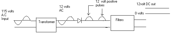
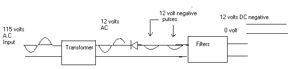
In the half wave power supply below the 115 volts input is stepped down to 12 volts by the transformer.
The diode passes the positive half of the 12 volt input but blocks the negative half resulting in 12 volt pulses.
The filters smooth these 12 volt pulses to almost pure DC.
1/2 wave power supply
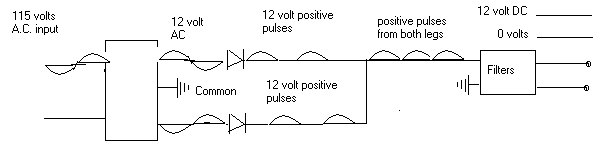
In the full wave power supply below the center of the transformer output or secondary winding is used
as the reference. At any instant in time the legs will be of opposite polarity from each other. As one
leg goes positive the diode in that leg conducts while the opposite leg is cut off by the negative voltage.
During the next half cycle the polarities are reversed and the other diode conducts while the first is cut
off by the negative voltage. As you can see this power supply makes use of twice the number of pulses
as the half wave above and is able to supply twice the current. With twice as many pulses the frequency
is also doubled compared to the half wave supply above making it easier to filter.
Full wave power supply
The diodes in the above circuits could be installed with opposite polarity to produce a
negative voltage output.
How do you determine if a diode is good or bad?
If you are using an older digital or an analogy multimeter you do a front to back check using the resistance
setting. Connect the meter leads and note the reading, then reverse the leads and again note the readings.
The reverse or high reading should be a least 10 times the forward or low reading.
The newer multimeters usually have a semiconductor test setting. Since these may function in
any one of several different ways please consult your manual.
********************************************************************************
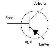
BIPOLAR TRANSISTORS
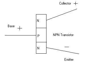
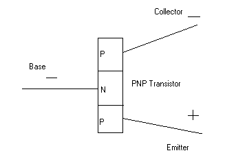
The drawings below illustrate the construction of common bipolar transistors. They come in two flavors
NPN and PNP types, the difference between the two is the polarity required. The NPN type is more
common then the PNP type simply because most equipments use a negative ground or common and a
positive supply or source.
I remember the polarities of each by starting with the Emitter lead:
TYPE- Emitter.......Base................Collector
NPN- Negative....Positive....More Positive
PNP- Positive....Negative...More Negative
The polarity applied to the COLLECTOR in most circuits is the same as that required
to forward bias the BASE circuit.
As you can see a transistor is made like a diode with an addition section added to it. A diode has
a single PN junction while a transistor has two, thus the name bi-polar. A diode will usually have
a 1N*** designation and a transistor a 2N***, however the imports may have a 2SC*** or
similar designation, other designations such as MRF*** and ECG*** are also used.
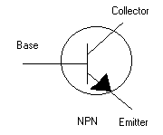
Below are the schematic symbols of both the NPN and PNP types. I remember which is which
using the the arrow on the emitter lead.
NPN- The arrow is: Not Pointing iN
PNP- The arrow is: Pointing iN from Perimeter
As with diodes, the voltages applied to the transistor are referred to as BIAS. The transistor
may be biased ON , OFF, More Than OFF, or somewhere in between these extremes.
There are three basic amplifier classes.
Class A- In a class A amp. current ("I") flows through the amplifying device all the time or 360 degrees
of the input cycle. The output wave form is an exact replica of the input wave form except larger and
shifted in phase by 180 degrees Often used in HI-FI audio amplifiers.
Class B- In a class B amp. the current ("I") flows in the amplifying device less than 360 degrees but more
than 180 degrees of the of the input cycle. The output wave form is not an exact replica of the input, but
is still useful for many purposes. Used in inexpensive audio equipment and some RF applications.
Class C- In a class C amplifier the current ("I") flows in the amplifying device for less than 180 degrees
of the input cycle. It is used almost exclusively in high efficiency RF amplifiers.
These amplifier classifications are used for both vacuum tube and transistor amplifiers.
There are also three basic transistor amplifier configurations:
Common Base
Common Collector
Common Emitter
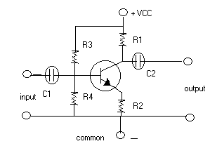
The names indicate which element of the transistor is common to both the input and output
circuits as you can see in the Common Emitter circuit below.
Common Emitter NPN Amplifier
The circuit above illustrates the most commonly used transistor amplifier configuration.
The arrow on the emitter lead tells us the this is a NPN (Not Pointing iN) Transistor.
Since we know that it is an NPN transistor in an amplifier circuit, we also know that the
Emitter is the most negative point of the transistor (not the circuit),
the Base will be more positive then the Emitter and
the Collector will be more positive than the Base when referenced to the Emitter.
A transistor may be thought of as a current ("I") controlled variable resistor.
Varying the input signal applied between the Base and Emitter leads results in a variation in the current ("I")
flow between the Collector and Emitter leads, similar to rotating the shaft of a variable resistor.
If you remember from the "series circuits" articles, the total of the voltage drops in a series circuit equal
the applied voltage. Varying the resistance of the transistor in the circuit above results in changes in the voltage
drops across R1,R2 and the transistor.
With no voltage applied across the Base/Emitter junction of the transistor, the transistor is cut off,
offering an extremely high resistance to current flow.
THIS IS A COMMON CHARACTERISTIC OF TRANSISTORS
and not unique to this circuit. Transistors are turn off until you turn them on.
This high resistance acts just as an infinitely high resistance (open circuit) in the circuit, thus the voltage or bias
measured between the Collector and bottom of R2 is the applied voltage.
THE BOTTOM OF R2 IS THE MOST NEGATIVE POINT OF THE CIRCUIT.
NEXT CONDITION
If the values of R3 and R4 are such that 0.7 volts (remember from the diodes) is applied between the Base and
the Emitter junction the transistor will be just at the verge of conducting.
( in theory anyway, transistors do vary a little, while one may still be cut off another from the same batch may
conduct a little)
If the input signal to this NPN transistor is made more negative, no change will be detected in the Collector/Emitter
circuit. An NPN transistor which is in cutoff as this one is can not be MORE cutoff.
If the input signal to this NPN transistor is made more positive the resistance in the Collector/Emitter circuit drops.
The transistor is no longer an infinitely high resistance and current flows in the circuit.
With current flowing in the circuit the voltage/bias measured between the Collector and Bottom of R2 will be less
than the applied voltage that we measured above.
With current flowing in the circuit, there will be an increase in the voltage drops across R1 and R2, remembering
that the total voltage drops must equal the applied voltage, the voltage drop across R1 will be same as the decrease
at the collector. As the input voltage is made more positive, more current will flow, and the voltage drop across R1
will increase, while the voltage drop across the transistor (and R2) will decrease.
If we continue to increase the positive bias between the Base/Emitter junction a point will be reached where the
transistor acts as a short circuit and no voltage is dropped between the Collector/Emitter junction.
(We would still measure a small voltage between the bottom of R2 and the Collector due to the
presents of R2 and it's voltage drop.)
These are the extremes in a transistor amplifier circuit:
The transistor is in "cutoff" acting as an infinite resistance, dropping the total applied voltage
at it's Collector,
or is in "saturation" acting as a short circuit with no voltage drop at it collector.
If measured at the output terminals we would see the voltage fluctuations of the Collector
as an AC signal(DC being blocked by C2), larger than the input signal and 180 degrees
out of phase with it.
Why use so many components?
Each component in this circuit serve a particular purpose.
C1 and C2 are the schematic symbols for capacitors.
Capacitors block DC potentials while allowing AC to pass insuring that the DC voltages of the
previous and the following stages of those circuits do not affect this circuit, while allowing the desired
AC input and output signals to pass. At the same time they keep the DC potentials of this circuit from
effecting the previous and following circuits.
R3 and R4 are resistors connected in series with each other and in parallel with the Collector/Emitter
circuit (which is composed of R1,R2 and the transistor) directly across VCC and common.
They compose a voltage divider circuit that is used to set the Base/Emitter bias which determines the
CLASS of operation of the transistor circuit.
If their values are chosen so that input signal can never drive the circuit into cutoff or saturation a
Class A amp. results. (360 degrees)
If chosen so that the circuit produces an output signal only on the forward biasing part of the input
signal, CLASS B operation results.(180 to 360 degrees)
If chosen so that the BASE is reverse biased, so that the input signal must first overcome this
reverse bias before causing the Collector/Emitter circuit to conduct, Class C operation is
achieved.(less than 180 degrees of the input)
Rule of thumb: the total value of R3 and R4 are chosen to be approx. 10 times the value of
R1 and R2.
R1 and R2 are chosen to limit the total current ("I") flowing in the Collector/Emitter circuit to a
value that does not exceed the transistors rating when it is driven into saturation.(shorted condition)
This would be the ideal situation but their values are more often chosen to allow more
"I" to pass, increasing the gain and linearity of the stage.
R2 the Emitter Resistor has a relatively low value. It's purpose is to keep the Emitter at a slightly
positive voltage referenced to common. Since forward biasing of the transistor requires that the Base
be more positive then the Emitter and transistors tend to conduct more and more as their temperature
increase, this slightly positive voltage helps to prevent " Thermal Runaway". As the transistor conducts
more, more current flows through R2 increasing the positive voltage at the Emitter keeping the
transistor from destroying itself in most situations. Often a capacitor is connected in parallel with this
resistor improving the gain of the stage by bypassing the AC component to common, partially eliminating
the affect of the DC voltage increase at the Emitter caused by R2 for the AC portion of the signal.
R1 the Collector Resistor is the other half of the voltage divider composed of itself and the transistor.
If R1 where to be removed from the circuit, the supply voltage would be seen at the Collector whether
the transistor was cutoff or saturated. With no voltage variation, there would be no output signal.
What would be the effect if we took the output from the top of R2 instead?
More Coming soon