 |
|
You can make printed circuit boards like this one at home for a modest expense. Invaluable to experimenters and homebrewers. |
|
|
|
You can make printed circuit boards like this one at home for a modest expense. Invaluable to experimenters and homebrewers. |
Why would anyone mess around to make PCB's?
I finally bit the bullet and tooled up to make my own circuit boards at home. The idea of hand-wiring some of the projects I'd like to do has kept me from even starting them. By making my own circuit boards I opened myself up to not only being able to create and re create favorite projects, but also much more complex projects. If you've done any kind of building at all, you can appreciate how much difference it makes to stuff a pre-printed PCB versus hand wiring on perfboard. It makes building some of the projects you see in magazines much more straightforward to do. Just convert the article's schematic to a board, buy the parts and put it together. Just a few steps short of a pre-kitted project.
Preliminary Stuff
While making PCB's at home isn't particularly difficult, it's not a trivial undertaking. You need to acquire some kind of PCB layout program, and build or buy some specialized equipment. There's also a bit of a learning curve to it, especially the PCB layout tool. There's nothing stopping you from using resist-pen, or even a simple computer paint program to define the traces. The downside is that this will limit you on the complexity of the circuit you can lay out, and make it harder to incorporate changes down the line.
PCB Layout Software
There's really no point in using the etch resist pen or paint program because a commercial-quality layout tool can be had for free. It's called EAGLE PCB, put out by CadSoft. You can download for free either a Linux or Windoze version of this layout tool, whose only limitation is a maximum of one schematic page and about a 2.5x4" PCB size. This is more than enough for most hobby/ham projects, and if you need more than that, the registered version cost is very reasonable. I run the Linux version and am very happy with it. Plan on spending a few (or more) evenings getting to understand the interface and component libraries, and you will see this is a much better solution than etch markers or paint programs.
Equipment Procurement
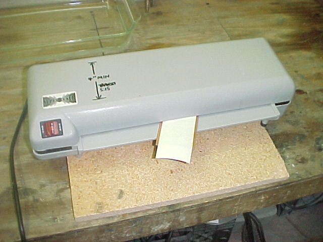
Depending on how resourceful you are, you can spend a little or a lot on etching equipment. I wimped out and bought most of my equipment but it wasn't hard to justify after seeing the results. I'm using what's known as the "toner transfer method", where you print your board layout onto a special paper using a laser printer, then "re-fuse" the toner onto a blank copper board using a laminating machine. Then you soak the paper off, leaving the toner behind. The etchant can't eat through the toner, so any copper covered with toner remains behind as circuit traces or component pads. Seems simple, and it is. But there are a few gotchas that will make or break the success of this process, so save yourself the grief that I went through and follow along below as we go through the process of making a board.
PCB Fabrication Process Details
| Here's where most projects end, before they ever get started, as a dry article in a ham magazine. The circuits on some of the more complex ones can be very time consuming to wire by hand. Sometimes the author may sell PCB's to accompany the article, but in my case I rarely want to build it exactly as shown. Making your own PCB's solves a lot of these problems. |
 |
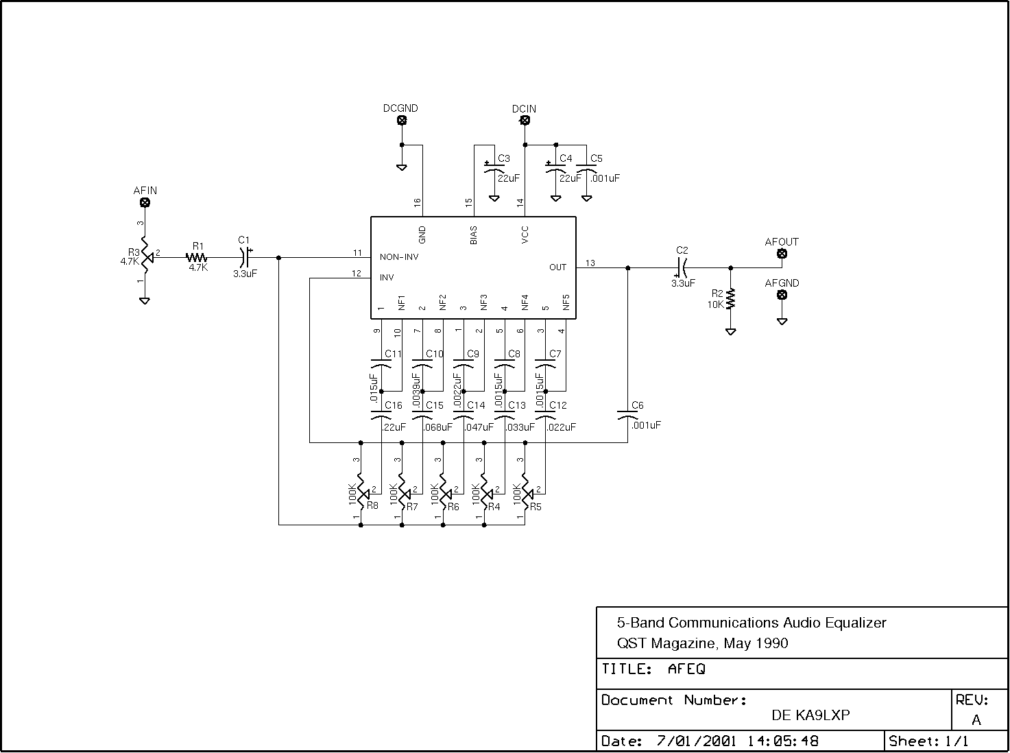 |
The first step is to transfer the schematic from the magazine to the schematic capture part of the layout program. I even try to use the same reference designators where possible so that I can reference back to the original article to make post-construction troubleshooting and parts correlation easier, if I have to. |

|
|
|
is used to place the parts on the board and route the copper traces. |
begins to clear up. If you're lucky, you get a PCB that requires no external jumper wires. |
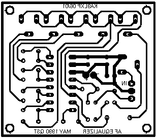
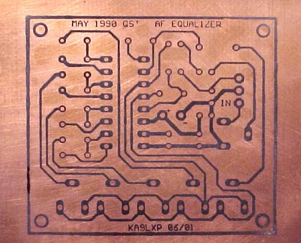
| When the layout is done, the board
layers are printed onto special toner transfer paper with a laser printer. This board "image" is transferred to the bare copper board with a laminating machine, or a hot clothes iron. |
|
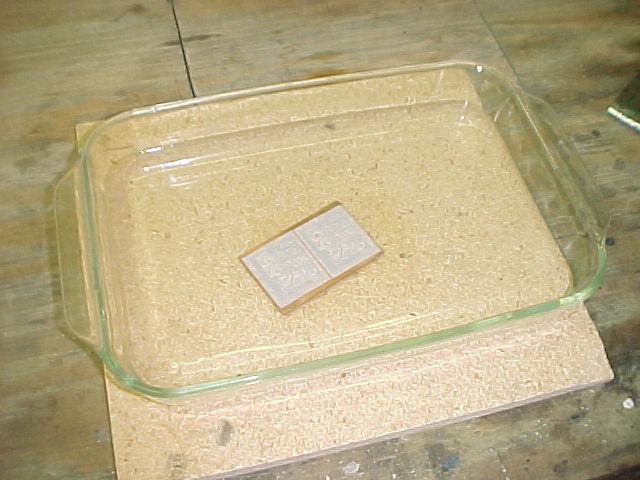 |
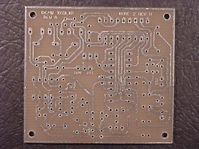
After laminating, the board with the
paper stuck to it is soaked to remove the paper, leaving only the toner behind. |
|
|
|
remaining, after the transfer paper has been soaked off. |
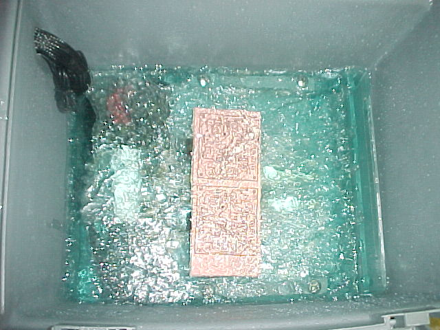
(Ammonium Persulfate) over the copper boards while two aquarium heaters keep the solution at 110F.This process can take anywhere from 10-30 minutes depending on the freshness of the solution and thickness of the copper. |
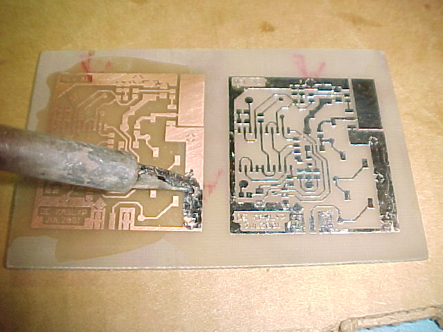
| After etching, the toner is removed with solvent and the board is tinned using a soldering iron and a small piece of tinned solderwick. Tinning isn't absolutely necessary but it improves the appearance of the board, and prevents the copper from oxidizing before it's time to solder the parts to the board. |
 |
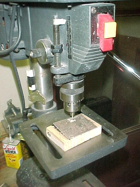 |
At this point, holes are drilled for any
leaded components and mounting holes. |
 |
|
|
 Back to the Main Project Page |
 Back to the K5LXP Home Page |
 � 2026 Pane Relief Computer Services |
|