|
Page last updated: 28/04/2013 |
50KHz Marker
Design
Simple design using readily available components.
Easy to build and set up.
Low power consumption suitable for battery operation.
A small and compact design.
Circuit description:
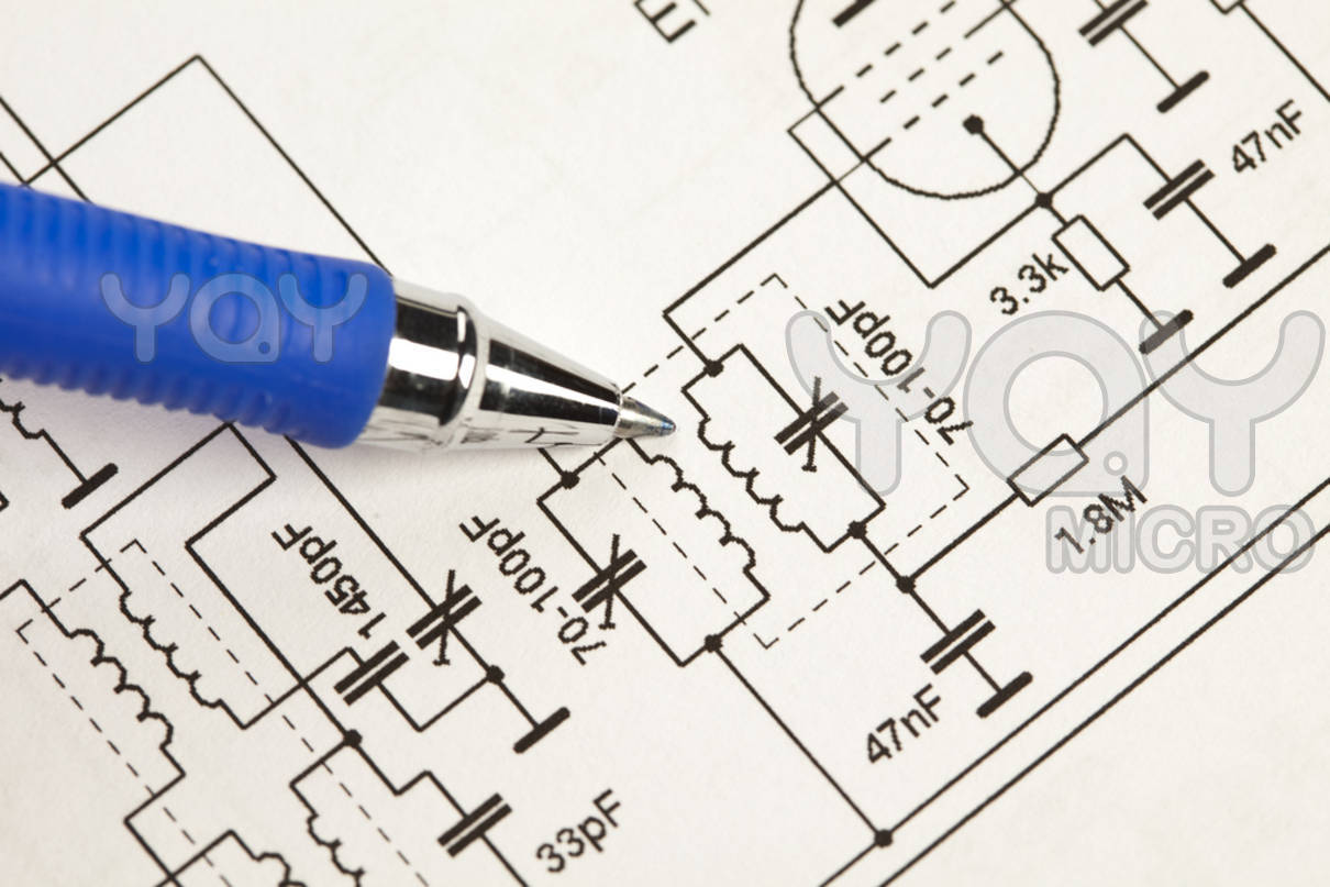
A simple to build, requiring no special test equipment or procedures to set, The circuit is presented here is pretty much build and go...
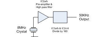
IC2 a quad 2 input NAND gate, IC2a forms an 8MHz crystal controlled oscillator buffered by IC2b, with C1 providing fine adjustment of the 8MHz reference. IC3 a dual 4 bit binary counter, IC3a IC3b IC2c and IC2d together form a fixed divided (divide by 160) providing a 100KHz square wave signal high in harmonic content at pin 9 of IC3 DC blocked by C3. IC1 a voltage regulator along with supply decoupling capacitors C4, 5, 6, & 7, provides a stable 5v supply to IC's 2 & 3 allowing the unit to be fed from a DC supply of between 7.5 and 35v.
 50KHz Marker PCB component placement / layout:
 50KHz Marker PCB bottom trace:
Original Files:
Further to the details of the pages above - the original CAD files created using EAGLE PCB Design software are included below, along with associated PDF files of both schematics and PCB layouts suitable for printing directly.
To use the original CAD files, they must be opened with EAGLE. Visit the CADsoft web site for more details, the software (including a freeware version), part libraries, tutorials, for EAGLE are available.
50KHz Marker PCB component layout PDF
50KHz Marker PCB bottom track layout PDF