QRO 23cm Harmonic Filter and
Reflectometer
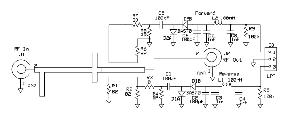
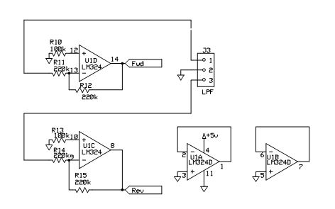
The circuit of the harmonic filter/reflectometer is shown above. The filter section consists of a quarter wave stub resonant at 2592MHz, and two stubs resonant at 3876MHz and 5184MHz spaced along the line so as to cancel the reactance of the lower frequency stub at 1296MHz. Each stub shorts out any harmonic energy and reflects it back towards the source. The reflectometer uses separate coupled lines for forward and reflected waves. With the component values shown the prototype forward detector produces just less than -5V for 600W forward power, whilst the reverse detector produces -1V for 60W of reflected power. The circuit below can be used to invert the signals for application to devices needing a +ve going signal such as PICs or Arduino controllers. A microcontroller can be used to linearise the power scale using a look up table or maths to solve a 2nd order polynomial fit.
Assembly
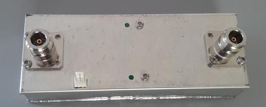
Start by marking out the box lid using the PCB as a guide
for the holes needed for J1, J2 and J3, making sure the PCB is centralised on
the lid as the clearances to the edges are tight. The central holes for J1 and
J2 need to be 6.5mm in diameter. When
the holes have been drilled and filed and any swarf
and sharp edges removed, make a trial assembly with
the N type sockets and PC forming a sandwich with the lid as the filling and
the PCB inside on the flanged side of the lid. Check that the box sides can be
fitted around the board and that the top cover can be fitted in place. Once any
necessary adjustments have been made, solder the box sides together and solder
the top lid (not the one with the PCB attached) to the box sides, using a
temperature controlled iron with a large bit. After the assembly has cooled,
check that the box can be removed/refitted from the
lid carrying the PCB. There may be some benefit in rigidity if additional
screws are placed as shown in the photo, on either side of the line near the
centre of the box, the holes for these can be drilled now.
At this stage the SMD components can be added to the PCB. Clean the PCB with a PCB cleaner before starting, you may find it beneficial to tin the component pads before adding the parts. Solder in the R’s and C’s first, then the two inductors and finish with the dual Schottky diodes D1 and D2. The DC output connector J3 may be added now. If you need to reduce the sensitivity of the reflectometer then there are pads provided to allow construction of attenuators using 0603 resistors. Calculation of the resistors needed should be based on a terminating impedance of 80 ohms for the line. Note that the diodes don’t look like a resistive termination, they exhibit mostly capacitive reactance, so simple voltage dividers can be used made from two resistors that add up to near 80 ohms.
Now measure the height of the centre pins of the N connectors above the PCB groundplane. Remove the connectors and carefully saw and file to leave 2.5mm protruding above the ground plane.
Enlarge the holes in the copper line to just fit over the N centre pins, increasing the drill diameter in stages and feeding the drill slowly to avoid damaging the line. File it if needed to get the alignment correct.
The line spacing required is 1.6mm above the groundplane to the underside of the line, easily jigged using odd scraps of FR4 PCB material. Clamp the line in place on the spacers then use a hot soldering iron to solder the line in place at each end. It should look like this:
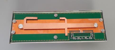
If you use small flange connectors with a thin centre pin, the holes in the line are the right diameter as supplied. You will need to drill additional holes through the flange into the box lid and PCB to accommodate fixing screws. Silver plated flanges of either size can be soldered to the box lid to ensure good grounding if you have a suitable soldering iron.
Tuning up
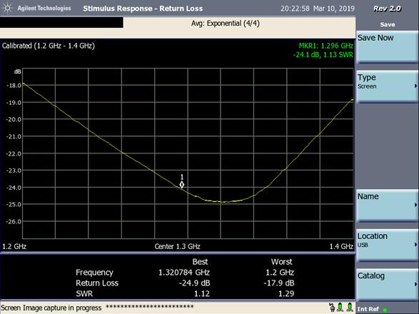
To tune up the filter you will need either a network analyser or a combination of spectrum analyser, signal generator, and a reflectometer bridge, The first stage is to check and adjust the in band return loss, using the set up in the figure below. By bending the line up or down a little in between the filter stubs it should be possible to achieve more than 25dB return loss at 1296MHz.

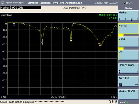
Having established the correct line impedance, then turn your attention to the stubs, starting with the longest one. This needs to be tuned to put a notch on 2592MHz. Using the set up below, start by looking over the range 2350MHz to 2850MHz to find the notch, then adjust the free end of the stub with pliers to tune it. Put the lid on the unit when measuring to ensure accuracy. The tuning is very sharp and may require some patience because the copper line is quite springy. Use a second pair of pliers and a piece of FR4 PCB as a spacer to hold the fixed end of the line firmly in place to make the process easier. Repeat this for the other two stubs, the shortest one should be tuned to 5184MHz and the intermediate one to 3876MHz. If you want to be sure you can then repeat the setting up process to get the best overall performance.

If you have a calibrated power measuring capability then you can check the reflectometer DC outputs using the intended transmitter and draw your own calibration chart. The prototype figures below give a guide to what you should see. Some typical performance graphs are included at the end.
|
Forward |
Reverse |
||
|
Power |
-DC
Out |
Power |
-DC
Out |
|
0 |
0 |
0 |
0 |
|
10 |
0.06 |
7 |
0.042 |
|
20 |
0.16 |
10 |
0.092 |
|
30 |
0.29 |
15 |
0.181 |
|
40 |
0.42 |
20 |
0.273 |
|
50 |
0.56 |
25 |
0.364 |
|
75 |
0.91 |
30 |
0.46 |
|
100 |
1.2 |
40 |
0.644 |
|
150 |
1.84 |
50 |
0.815 |
|
200 |
2.3 |
60 |
0.97 |
|
250 |
2.72 |
|
|
|
300 |
3.08 |
|
|
|
350 |
3.45 |
|
|
|
400 |
3.73 |
|
|
|
450 |
4.05 |
|
|
|
500 |
4.35 |
|
|
|
550 |
4.64 |
|
|
|
600 |
4.88 |
|
|
If you need any help then please email me ([email protected]).
Component List
Laser cut copper line G3XDY
Groudplane/Reflectometer PCB G3XDY
Tin Box 55.5x148x30 No1000107 G3NYK
N type connectors J1/J2 eg G0KSC on EBay
These must have a completely flat back. The reduced
flange type may be used if suitable holes are drilled in the PCB.
R1 82
ohm 0603 SMD G3XDY
R2 82 ohm 0603 SMD G3XDY
R3 0 ohm link 0603 SMD G3XDY
R4 Not required
R5 100k ohm 0805 SMD G3XDY
R6 82 ohm 0603 SMD G3XDY
R7 39 ohm 0603 SMD G3XDY
R8 39 ohm 0603 SMD G3XDY
R9 100k ohm 0805 SMD G3XDY
C1 100pF 50V 0603 SMD G3XDY
C2 100pF 50V 0805 SMD G3XDY
C3 1nF 50V 0805 SMD G3XDY
C4 1nF 50V 0805 SMD G3XDY
C5 100pF 50V 0603 SMD G3XDY
C6 100pF 50V 0805 SMD G3XDY
C7 1nF 50V 0805 SMD G3XDY
C8 1nF 50V 0805 SMD G3XDY
L1 100nH 0805 SMD G3XDY
L2 100nH 0805 SMD G3XDY
J3 3 pin 0.1” KK plug G3XDY
D1A,B BAS70-04 G3XDY
D2A,B BAS70-04 G3XDY
Hardware: M3 stainless steel screws 8mm long and M3 stainless steel nuts