 UNMODIFIED
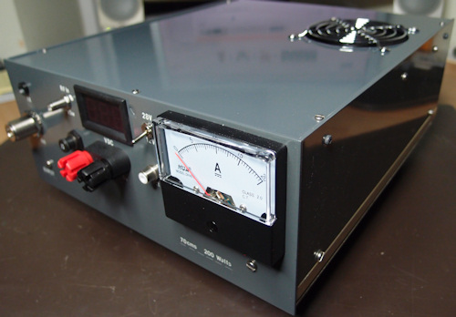 G3WZT VERSION
NOTES
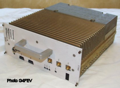
1] Remove and discard all boards except the main PA and receiver boards. I left my board complete as I wanted to use the heat sink as supplied.
It is important to either remove the complete PA board from the heatsink, or remove the PA output FETs so that new heat sink compound can be applied to them. Mine were totally dried out and needed a new application. Poor heat sinking of these parts at these power levels will lead to certain "death" by thermal failure.
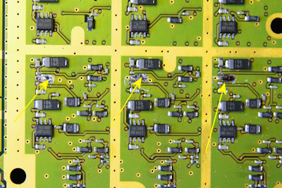
2] PA and Driver Bias modifications shown on the link given above are perfectly adequate but bear in mind that originally this unit had software controlled bias and the simple "adjustable pot" modifications are not temperature compensated and DO drift when the unit gets hot. Adjust the bias for the correct value and after the heat-sink has warmed up, readjust again for the correct bias values. There is no need to lift the Drain connections to set up, just measure the 28V DC current and adjust the bias for an increase of the requires amount. The correct Drain current is 160mA for each half of each PA FET, ie 320ma for each push pull package (640ma total for the output stages). IDQ for the driver stage, if used, is 40mA. However it should be noted that the driver stage is NOT able to deliver sufficient drive power to fully drive the output stage to its full potential. Around 25W drive will be needed for 200 Watts output from the unit.
NB RF input and output MUST be terminated into 50 ohms when setting bias current to prevent possible instability.
 DRIVER
BIAS
DRIVER
BIAS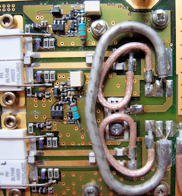 PA BIAS MOD.
3] The unit requires 2 supply voltages, 28V and 12V DC. 28V is supplied on a separate pin (p6) for the driver stage and if this is not going to be used simply leave that pin unused. 28V for the BLF548 PA output stage is applied to the first 2 pins on the connector (P 2 and 4).
+12V DC is applied to pins 14 and 16. Ground is on pins 8, 10, 12, 18, 20, 24, 26, and 28.
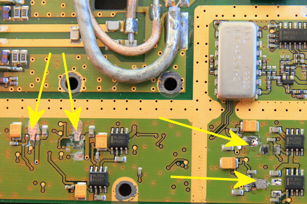
4] With just the PA board installed, the +12V current is in excess of 1 Amp, this means that a TO220 regulator cannot be used from the +28V supply unless this current is reduced. Much of this is drawn from the receivers and other ICs on the board. I reduced mine to 182mA and have fitted a 7812 regulator for the 12V supply fed from the main 28V supply. This is shown in the photo's below next to the existing +8V regulator. All other regulators are not required and may be removed.
Reduction in 12V DC current may be achieved by removing the SMD regulators on the board and lifting the 12V supply filter. I have included photos of the items removed. It is quite easy to determine where the power is being wasted by simply placing the side of your hand on the components and noting what is getting warm! When the 12V current is less than 200mA an LM7812 may be fitted a shown below.
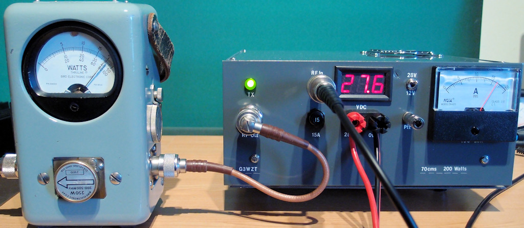
4] Depending on the drive level you have available the unit can be used with or without the driver and pre-driver. I tested mine with and without the BLF544 driver but not with the low level pre driver stage (BLF521). Input to the driver is a very good 50 ohm match and mine required onlt 0.5-1W of drive for full output but this was limited to around 140 Watts due to saturation of the driver stage. 200 Watts output is comfortably obtained by driving the output stage only, with around 25 Watts at the input.
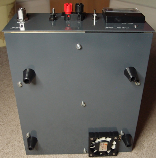
Please note warnings given elsewhere regarding the power rating of the Sageline 3dB output combiner; it does get hot at these levels as it was designed for lower power output levels and needs to be cooled. You will see from the photo left, that I have arranged a small blower directly onto the output combiner in my unit. This only runs on transmit.
When using the output stage only, I did observe instability when the input was left unterminated. This is evident as excessive drain current when the bias has been set and the unit is in the transmit mode. In my case around 8 Amps which is rather undesirable. It is perfectly stable when correctly terminated.
For this reason I consider that correct sequencing of the antenna changeover relays and supplies is essential. With correct sequencing the input and output will be correctly terminated before the amplifier is put into transmit mode. On my unit +28V is left on all of the time and the +12V correctly sequenced supply is switched between transmit and receive. With enhancement mode FETs this is quite normal practice as there is no gate bias when the 12V is off.
For sequencing I used a "TROPIC" board designed by GW4GTE at S9PLUS.com this is an excellent product at a very fair price and does all that is needed for this project plus much more if needed.
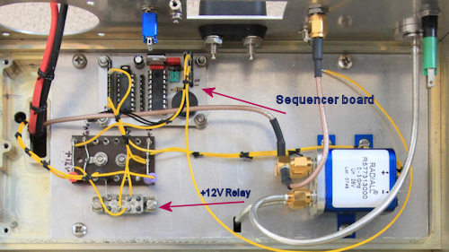
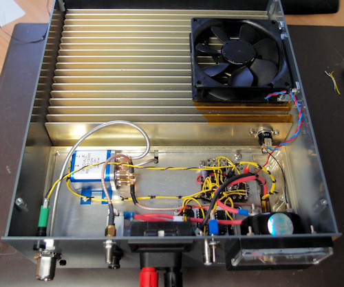
In this view, the "TROPIC" sequencer board can be seen along with the 12V supply relay used to switch between receive and transmit. The RF input and RF output are both switched using a Radial coaxial transfer relay.
This relay, along with the 12V supply relay are both switched from the "Tropic" sequencer board. If required the Tropic will sequence up to 5 outputs; it also has 2 interlock or inhibit pins which may be used, for example, as VSWR shutdown protection.
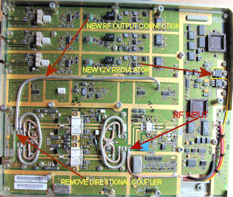
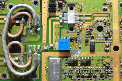
The PA board is shown here as I have implemented it. The output coupler has beed removed and a new RF output coax fed out through the board.
RF input to the PA output stage is made where shown and provides a good 50 ohm match. The PA driver stage is left intact although it is not used. Providing 28V is not supplied to pin 6 of the edge connector, this stage will not have drain voltage applied.
The heatsink cooling fan runs via a 50 degree thermal switch.
1] Remove and discard all boards except the main PA and receiver boards. I left my board complete as I wanted to use the heat sink as supplied.
It is important to either remove the complete PA board from the heatsink, or remove the PA output FETs so that new heat sink compound can be applied to them. Mine were totally dried out and needed a new application. Poor heat sinking of these parts at these power levels will lead to certain "death" by thermal failure.
2] PA and Driver Bias modifications shown on the link given above are perfectly adequate but bear in mind that originally this unit had software controlled bias and the simple "adjustable pot" modifications are not temperature compensated and DO drift when the unit gets hot. Adjust the bias for the correct value and after the heat-sink has warmed up, readjust again for the correct bias values. There is no need to lift the Drain connections to set up, just measure the 28V DC current and adjust the bias for an increase of the requires amount. The correct Drain current is 160mA for each half of each PA FET, ie 320ma for each push pull package (640ma total for the output stages). IDQ for the driver stage, if used, is 40mA. However it should be noted that the driver stage is NOT able to deliver sufficient drive power to fully drive the output stage to its full potential. Around 25W drive will be needed for 200 Watts output from the unit.
NB RF input and output MUST be terminated into 50 ohms when setting bias current to prevent possible instability.
DRIVER
BIASPA BIAS MOD.3] The unit requires 2 supply voltages, 28V and 12V DC. 28V is supplied on a separate pin (p6) for the driver stage and if this is not going to be used simply leave that pin unused. 28V for the BLF548 PA output stage is applied to the first 2 pins on the connector (P 2 and 4).
+12V DC is applied to pins 14 and 16. Ground is on pins 8, 10, 12, 18, 20, 24, 26, and 28.
4] With just the PA board installed, the +12V current is in excess of 1 Amp, this means that a TO220 regulator cannot be used from the +28V supply unless this current is reduced. Much of this is drawn from the receivers and other ICs on the board. I reduced mine to 182mA and have fitted a 7812 regulator for the 12V supply fed from the main 28V supply. This is shown in the photo's below next to the existing +8V regulator. All other regulators are not required and may be removed.
Reduction in 12V DC current may be achieved by removing the SMD regulators on the board and lifting the 12V supply filter. I have included photos of the items removed. It is quite easy to determine where the power is being wasted by simply placing the side of your hand on the components and noting what is getting warm! When the 12V current is less than 200mA an LM7812 may be fitted a shown below.
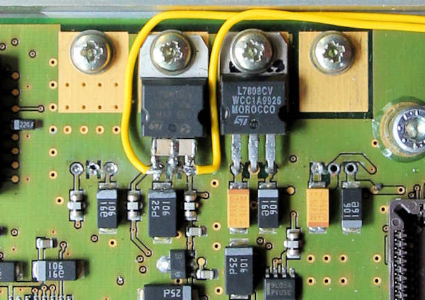
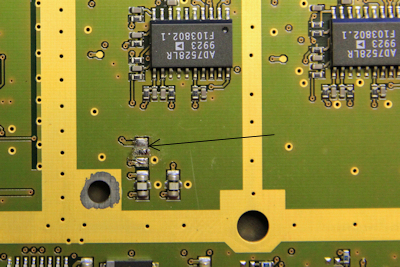
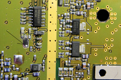
REMOVE ALL OF THE COMPONENTS SHOWN WITH
AN ARROW TO REDUCE THE 12V POWER CONSUMPTION
4] Depending on the drive level you have available the unit can be used with or without the driver and pre-driver. I tested mine with and without the BLF544 driver but not with the low level pre driver stage (BLF521). Input to the driver is a very good 50 ohm match and mine required onlt 0.5-1W of drive for full output but this was limited to around 140 Watts due to saturation of the driver stage. 200 Watts output is comfortably obtained by driving the output stage only, with around 25 Watts at the input.
Please note warnings given elsewhere regarding the power rating of the Sageline 3dB output combiner; it does get hot at these levels as it was designed for lower power output levels and needs to be cooled. You will see from the photo left, that I have arranged a small blower directly onto the output combiner in my unit. This only runs on transmit.
When using the output stage only, I did observe instability when the input was left unterminated. This is evident as excessive drain current when the bias has been set and the unit is in the transmit mode. In my case around 8 Amps which is rather undesirable. It is perfectly stable when correctly terminated.
For this reason I consider that correct sequencing of the antenna changeover relays and supplies is essential. With correct sequencing the input and output will be correctly terminated before the amplifier is put into transmit mode. On my unit +28V is left on all of the time and the +12V correctly sequenced supply is switched between transmit and receive. With enhancement mode FETs this is quite normal practice as there is no gate bias when the 12V is off.
For sequencing I used a "TROPIC" board designed by GW4GTE at S9PLUS.com this is an excellent product at a very fair price and does all that is needed for this project plus much more if needed.
In this view, the "TROPIC" sequencer board can be seen along with the 12V supply relay used to switch between receive and transmit. The RF input and RF output are both switched using a Radial coaxial transfer relay.
This relay, along with the 12V supply relay are both switched from the "Tropic" sequencer board. If required the Tropic will sequence up to 5 outputs; it also has 2 interlock or inhibit pins which may be used, for example, as VSWR shutdown protection.
The PA board is shown here as I have implemented it. The output coupler has beed removed and a new RF output coax fed out through the board.
RF input to the PA output stage is made where shown and provides a good 50 ohm match. The PA driver stage is left intact although it is not used. Providing 28V is not supplied to pin 6 of the edge connector, this stage will not have drain voltage applied.
The heatsink cooling fan runs via a 50 degree thermal switch.