|  |  |  |  |  |  |  |  |  |  |  |  |  |  |  |  |  | 
   
    |  | A 
        SIGNAL SOURCE IS THE FIRST STEP... ... |  | 
   
    |  |  |  |  |  |  |  |  |  |  |  |  |  |  |  |  | 
   
    |  | General 
      description ... ... |  | 
   
    |  |  |  |  |  |  |  |  |  |  |  |  |  |  |  |  | 
   
    |  | 
         
          |   On our work bench, signal souce is 
              a necessary tool for experiment and adjustment. The synthesizer 
              here we described is versatile enough for common usage. It has two outputs:  A: Main output 0 -> 500MHz in 0.25Hz 
              step Main A: 0 -> 500MHz -2dBm ouput Main B: 0 -> 125MHz +10dBm output B: Sub-output 1050 -> 1075MHz in 
              50KHz step   |  |  |  |  |  |  | 
   
    |  |  |  |  |  |  |  |  |  |  |  |  |  |  |  |  | 
   
    |  | The 
      AD985x series DDS IC provides the designer an easy way of synthesizer designing. 
      Out of this DDS family, the AD9858 is the fastest one, which can run under 
      2GHz. When we 
      use this IC in our design, we find that some technical issue in the datasheet 
      should be emphasized more so that the user can understand more thoroughly. |  |  |  | 
   
    |  |  |  |  |  |  |  |  |  |  |  |  |  |  |  |  | 
   
    |  |  
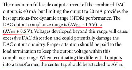
        All 
          the other members in this family, like AD9850/51, 52/53, have a sourcing 
          current DAC. Only the AD9858 uses a sinking current DAC, this is an 
          important issue in application. For a sourcing current DAC, the user 
          connects the loading resistor to AGND. But for a sinking current DAC, 
          the user should connect the loading resistor to AVDD. There are two 
          places in the datasheet mention that design point, but none is direct. 
          You will find the following parameters in the datasheet: |  |  |  | 
   
    |  |  |  |  |  | 
   
    |  |  |  |  |  |  |  |  |  |  |  |  |  |  |  |  | 
   
    |  | In 
        the "Electrical Specification" Table, the "Voltage Compliance 
        Range" parameter indicates that the DAC loading resistor should connect 
        to the AVDD, but that description is not clear enough.  |  |  |  | 
   
    |  |  |  |  |  |  | 
   
    |  |  |  |  |  |  |  |  |  |  |  |  |  |  |  |  |  |  | 
   
    |  |  |  | 
         
          |  |  |  |   
          |  Also, 
              this paragraph mentions the terminating using transformer but does 
              not describe single end usage. Unfortunately, there is neither a 
              typical application circuit included in this document, nor evaluation 
              board schematic available on the web. So user may feel strange when 
              they connect the output stage as same as the AD9852's, but it does 
              not work.
 |  |  |  |  |  | 
   
    |  |  |  |  |  |  |  |  |  |  |  |  |  |  |  |  |  |  | 
   
    |  |  |  | So 
        it's better to add a direct description of the DAC output stage, and make 
        it clear that the DAC sinks current. That means the loading resistor should 
        connect to AVDD. Or, of cause, an application schematic is the best method 
        to express that:  |  |  |  | 
   
    |  |  |  |  |  |  |  |  |  |  |  |  |  |  |  |  |  |  | 
   
    |  |  |  | 
         
          |  |  |  
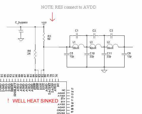
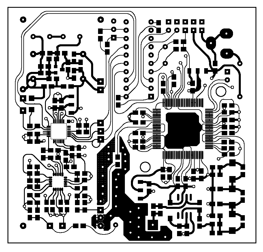
              The second issue is also showed in the left diagram. This IC should 
              be WELL HEAT SINKED! When operating under 2GHz, this IC produces 
              high temperature. It's dangerous if the PCB design is not optimized 
              or the IC's substrate metal is not well soldered to the PCB. Dissipating 
              2W of heat through PCB VIAs and GROUND PLANE sometimes sounds not 
              practical. So it's necessary to add extra heat sink on the top of 
              the IC. So we think it's better to hint the user in the datasheet. |  |  |  |  | 
   
    |  |  |  |  |  |  |  |  |  |  |  |  |  |  |  |  |  |  | 
   
    |  |  |  | AND 
      HERE WE BEGIN ... ... |  |  |  | 
   
    |  |  |  |  |  |  |  |  |  |  |  |  |  |  |  |  |  |  | 
   
    |  |  |  | 
         
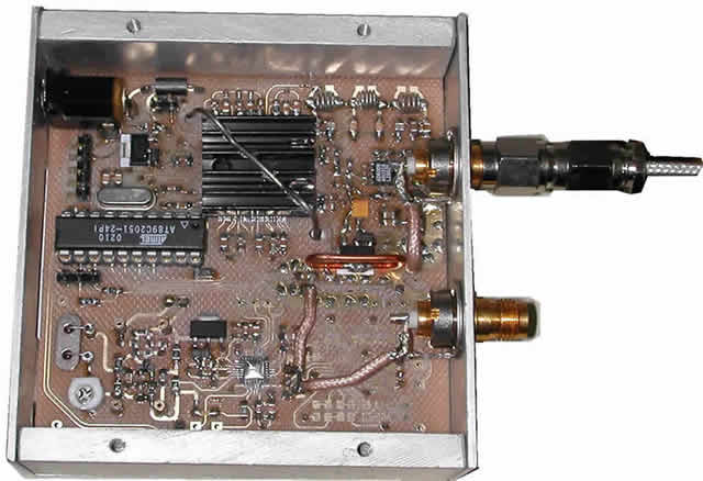
          | We 
            feed the AD9858 with a 1G synthesized source. The chip we use here 
            is LMX2532 from National Semiconductor, 
            and it's well suited for this job. The frequency range of this IC 
            is 1052MHz to 1077MHz. We set the default frequency to 1,073,741,824Hz, 
            which is 0.25 x 2 ^ 32, so we can set tuning step at 0.25Hz. But a 
            0.25Hz tuning step is not practical at all, unless you got a ATOMIC 
            clock reference. |  |  |  |  |  |  | 
   
    |  |  |  |  |  |  |  |  |  |  |  |  |  |  |  |  |  |  | 
   
    |  |  |  | 
         
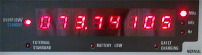
          |  |  | This 
            is the PLL output frequency we measured at the reference output after 
            5 minutes. And you can see that the frequency drifts to 1,073,741,050Hz. 
            The crystal we use has a temperature coefficient of about -1ppm, and 
            that will cause large drift at 1GHz. |  |  |  |  | 
   
    |  |  |  |  |  |  |  |  |  |  |  |  |  |  |  |  |  |  | 
   
    |  |  |  | In 
      another article, I will describe how to design an ovenized crystal oscillator. 
      Using a well designed ovenized oscillator we can obtain a +/-0.05ppm drifting 
      performance. If this project is just for common testing or transceiver excitation, 
      a temperature compensated oscillator is enough. |  |  |  | 
   
    |  |  |  |  |  |  |  |  |  |  |  |  |  |  |  |  |  |  | 
   
    |  |  |  | The 
      output of the PLL is splitted into two branchs. One is fed into the reference 
      clock input of AD9858. To obtain better clock feed through performance, 
      we add a 10dB attenuator before the AD9858 input. The other branch is an 
      MMIC output buffer for reference output. The MMIC here we use is NEC 
      upc1677, and also there is a design note for this part of circuit. |  |  |  | 
   
    |  |  |  |  |  |  |  |  |  |  |  |  |  |  |  |  |  |  | 
   
    |  |  |  | 
         
          | TIPS: |  | To 
            get the best performance of LMX2532, both digital and analog power 
            supply should be well regulated and filtered. Here we use an AS1117 
            to get 3.3V from 5.0V main voltage. The bypass capacitors consist 
            of some 1uF,1nF and 100pF chip caps. They are placed as near as posible 
            to the PLL IC. |  |  |  |  | 
   
    |  |  |  |  |  |  |  |  |  |  |  |  |  |  |  |  |  |  | 
   
    |  |  |  | The 
      programming of LMX2532 and AD9858 is an easy job. We use an AT89C2051 to 
      do that. On the control board, we use a software simulated SPI interface 
      for inter-board communication. Because this module is often used as tracking 
      generator for my home made spectrum analyzer. |  |  |  | 
   
    |  |  |  |  |  |  |  |  |  |  |  |  |  |  |  |  |  |  | 
   
    |  |  |  | Analog 
      Device recommends that in order to get the best 
      SFDR, the output current of the DAC can't be too large. And it's true, in 
      fact, 20mA is too large. We set it to 10mA, and use an AD8009 to amplifier 
      the output to a wanted level. |  |  |  | 
   
    |  |  |  |  |  |  |  |  |  |  |  |  |  |  |  |  |  |  | 
   
    |  |  |  | 
         
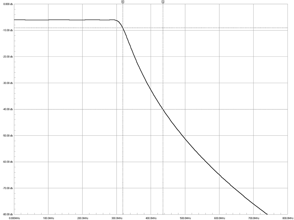
          | Here 
            is another key issue, the output filter. 
            Analog Device calls it a "construction filter", and my DSP 
            friends call it an "anti aliasing filter". Anyway, whatever 
            it's called, it is DO important. For a DDS IC operating under such 
            a high frequency, the output spectrum consists of harmonics, aliasing, 
            and clock feed through. |  |  |  |  |  |  | 
   
    |  |  |  |  |  |  |  |  |  |  |  |  |  |  |  |  |  |  | 
   
    |  |  |  | So 
      a well designed 7th elliptical filter is a MUST. We make an elliptical design 
      first, but some capacitors are too "odd" to find or combine. Then 
      we finally use a 7th chebyshev filter. |  |  |  | 
   
    |  |  |  |  |  |  |  |  |  |  |  |  |  |  |  |  |  |  | 
   
    |  |  |  | Here 
      is the simulated frequency response of the filter: |  |  |  |  |  |  |  | 
   
    |  |  |  |  |  |  |  |  |  | 
   
    |  |  |  |  |  |  |  |  |  |  |  |  |  |  |  |  |  |  | 
   
    |  |  |  | In order to be adaptable 
      with most loading impedance, we use a 1GHz/Gain*Bw OpAmp-AD8009 as output 
      buffer. This IC has superb spurious performance. We set the gain to 4, and 
      the corresponding band width is about 330MHz. |  |  |  | 
   
    |  |  |  | 
         
          |  |   
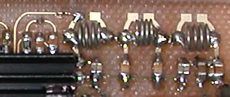
          | Some 
            TIPS: For most RF project, 
            the inter-connection between differents functional blocks is done 
            with RF shielding cable. For better performance, a double-shielding 
            low-loss Teflon cable is prefered. |   
          |  |   
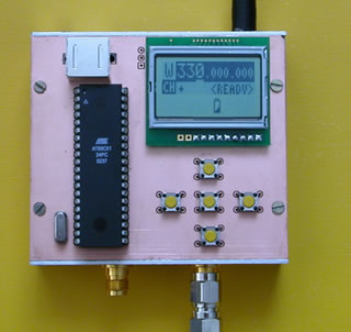
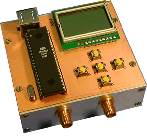
          | OK, up to now, 
            nearly everything has been done. Except the control unit. In fact, 
            the control unit is also important, because we always use this signal 
            source as track-gen of a SA. So this "slave" 
            must understand what the "master" 
            want it to do. |   
          |  |  |  |  |  |  |  | 
   
    |  |  |  |  |  |  |  |  | 
   
    |  |  |  |  |  |  |  |  | 
   
    |  |  |  | OK, let's take 
      a look of the control unit and the user interface... |  |  |  | 
   
    |  |  |  |  |  |  |  |  |  |  |  |  |  |  |  |  |  |  | 
   
    |  |  |  |  |  |  |  | 
         
          | Here is what it looks like. It consists 
              of: A: A graphical LCD 
              display B: Five-key keyboard C: A SPI serial interface |   
          |  |   
          | The graphical LCD displays the frequency, 
              sweep mode and modulation mode etc.  
              The five keys are:  
                Left_shift,Mode,Right_shift,Inc and Dec. In fact, it's more convinient 
                to use a ten-number keyboard together with a rotary encoder. |   
          |  |  |  |  |  | 
   
    |  |  |  |  |  |  |  |  |  |  |  |  |  |  |  |  |  |  | 
   
    |  |  |  | I will describe 
      the control method later. After fully assembled, the generator looks like: |  |  |  | 
   
    |  |  |  |  |  |  |  |  |  |  |  |  |  |  |  |  |  |  | 
   
    |  |  |  | 
         
          | Although 
            we don't use it as an instrument, we also need to do a thurough test 
            of the performance. |   
          |  |   
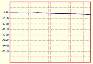
          | First, we measure 
            the output amplititude and amp/frequency flatness. |   
          |  |   
          | For main A 
            output, the average output is -2dB+/- 0.3dB, there is a little attenuation 
            at the high frequency range around 500 MHz, which is caused by the 
            FR4 PCB's material loss. |  |  |  |  |  |  | 
   
    |  |  |  |  |  |  |  |  |  |  |  |  |  | 
   
    | TO 
      BE CONTINUED ... ... |  |  |  |  |  |  |  |  |  |  |  |  | 
   
    |  |  |  |  |  |  |  |  |  |  | 
   
    |  |  |  |  |  |  |  |  |  |  | 
   
    |  |  |  |  |  |  |  |  |  |  |  |  |  |  |  | 
   
    |  |  |  |  |  |  |  | The AD8009 is not 
      capable of handling 10dBm output with single +5V power supply for frequency 
      above 120MHz, so we add a 5-pole LPF with cut-off frequency of 125MHz before 
      and post the AD8009. Thus the flatness measurement for main B output is 
      only applied upto 120MHz. |  |  |  | 
   
    |  |  |  |  |  |  |  |  |  |  |  |  |  |  | 
   
    |  |  |  |  |  |  |  |  |  |  |  |  |  |  |  |  |  | 
   
    |  |  |  |  |  |  |  |  |  |  |  |  |  |  |  |  |  |  | 
   
    |  |  |  |  |  |  |  |  |  |  |  |  |  |  | 
   
    |  |  |  | 
         
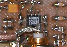
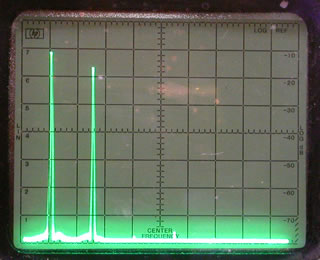
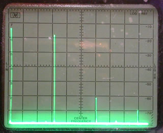
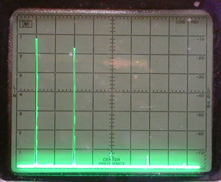
          | Also we need to know the 
              SFDR (Spurious Free Dynamic Range). To implement that measurement 
              we use a HP85?? spectrum analizer. For output main A, the 
              wide band SFDR is no worse than -45dBc for full frequency range 
              from 10Hz to 500MHz. For frequency below 180MHz and above 300MHz, 
              the SFDR is better than -55dBc. For outputmain B, the 
              SFDR is quite similar to main A, because we limit the maximum frequency 
              below 120MHz. Further more, if you use complementary power supply 
              of +/- 5V for the AD8009, the result could be even better. |  |  |  |  |  |  | 
   
    |  |  |  |  |  |  |  |  |  |  |  |  |  | 
   
    |  |  |  |  |  | Figure 
      1: -2dBm,30MHz Main A output..... ...(20M/div,10dB/div,100KHz band width) |  |  |  | 
   
    |  |  |  |  |  |  |  |  |  |  |  |  |  |  |  |  |  |  | 
   
    |  |  |  |  |  |  |  |  |  |  |  |  | 
   
    |  |  |  |  |  |  |  |  |  |  |  |  |  |  |  |  |  |  | 
   
    |  |  |  | Figure4: 
      -2dBm,30MHz Main B output..... ...(10M/div,10dB/div,300KHz band width) |  |  |  |  | Figure 
      2: -2dBm,50MHz Main A output..... ...(20M/div,10dB/div,100KHz band width) |  |  |  | 
   
    |  |  |  |  |  |  |  |  |  |  |  |  |  |  | 
   
    |  |  |  | 
         
          | Note that the AD8009 produces 
              significant 2nd and 3rd order harmonics. * In all 
              the figures, the left vertical line is the 0Hz reference.  * For 
              main B output, the signal is attenuated by 20dB before fed into 
              the Spectrum analizer. |  |  |  |  |  |  |  |  | 
   
    |  |  |  |  |  |  |  |  |  |  |  |  |  | 
   
    |  |  |  | Construction detail 
      of the 500MHz Low Pass Filter: |  |  |  |  | 
   
    |  |  |  |  |  |  |  |  |  |  |  |  |  | 
   
    |  |  |  |  |  |  |  |  |  |  |  | 
   
    |  |  |  |  |  |  |  |  |  |  |  |  |  |  |  | 
   
    |  |  |  |  |  |  |  | Figure 3: -2dBm,100MHz Main 
        A output.... ...(50M/div,10dB/div,300KHz band width) |  |  |  | 
   
    |  |  |  |  |  |  |  |  |  |  |  |  |  |  |  | 
   
    |  |  |  |  |  |  |  |  |  |  |  | 
   
    |  |  |  |  |  |  |  |  |  |  |  |  |  | 
   
    |  |  |  |  |  | And the 125MHz Low Pass Filter. |  |  |  |  | 
   
    |  |  |  |  |  |  |  |  |  |  |  |  |  | 
   
    |  |  |  |  |  |  |  |  |  |  |  |  |  |  |  |  |  |  | 
   
    |  |  |  | The PCB artworks 
      -- TOP layer--Bottom 
      layer--Silkscreen |  |  |  |  |  |  | 
   
    |  |  |  |  |  |  |  |  |  |  |  |  |  |  |  |  |  |  | 
   
    |  |  |  |  |  |  |  |  | 
   
    |  |  |  |  |  |  |  |  |  |  |  |  |  |  |  |  |  |  |