 |
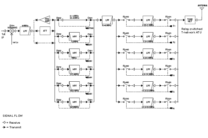
Figure 1 is a highly-simplified excerpt from the IC-703 block diagram. It shows the PA low-pass filters (LPF), TX/RX high-pass filters (HPF), switchable RX preamp and attenuator and RX 1st mixer/TX final mixer. Only the HF range (exclusive of 6m) is shown here.
In a compact, portable or mobile transceiver such as the IC-703, IC-706 or IC-7000, the sharing of subsystems between transmit and receive functions (where possible) is highly advantageous, as it reduces component count, internal real-estate requirements and ultimately, cost. The conventional scheme uses common diode-switched bandpass filters (BPF) in the receiver front end and exciter output stage. In these compact radios, the BPF function is split between the existing PA low-pass filters (LPF) and a bank of simpler high-pass filters (HPF)*. This has several advantages:
The PA low-pass filters carry the full RF output of the transmitter, and are thus relay-switched. As these filters are closest to the antenna, re-using them as the receiver's first RF filter stage eliminates switching or PIN diodes from the RF signal path of the receiver. Switching diodes can generate shot noise, and also create IMD products under strong-signal conditions; PIN diodes insert loss ahead of the first active RF stage, thus degrading system NF. It is noteworthy that all high-end commercial and military HF transceivers use relay-switched RF bandpass filters - as do some amateur transceivers such as the IC-7700, the IC-7800 and the Elecraft K2. The use of relay switching can significantly improve IMD2 and IMD3 dynamic range.
As the PA LPF inductors are physically larger so as to carry the transmitter's relatively high RF currents without saturation or excessive loss, their Q will be higher. This will sharpen the filter roll-off, thus improving the skirt selectivity of the LPF/HPF combination. The larger cores will be less likely to saturate (another IMD source) at high signal levels.
Whilst not as effective as a relay-switched BPF array, this configuration can reduce IMD due to strong signals above the cutoff frequency of the selected LPF, and reduce the likelihood that the switching diodes in the HPF's behind the LPF array will generate IMD.
An internal or external ATU (antenna tuning unit) will provide some additional RF preselection. Typically, the ATU is a T-network, and behaves as a high-pass filter. As in the PA LPF, the ATU inductor has a fairly high Q to minimise insertion loss. Cascading the ATU and the PA LPF will yield an RF bandpass filter with fairly steep skirts; the additional tuned stage right at the antenna will reduce even further the probability of IMD due to downstream switching diodes. In the IC-703, it is advantageous to leave the ATU activated at all times. The same effect can be achieved with the IC-7000 by placing the IC-AT180 or equivalent in the HF feedline.
* The second-order intercept (IP2) of the IC-703 would have been higher if separate 10 and 14 MHz HPF's had been provided.
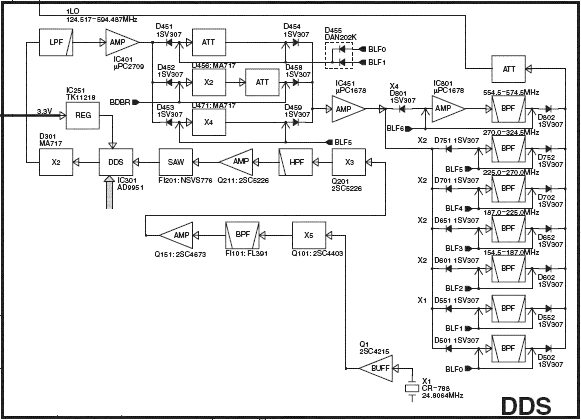 |
Figure 2 is a simplified representation of the DDS 1st LO (local oscillator) subsystem, from the IC-7000 block diagram. This design represents a radical departure from the conventional DDS/PLL architecture which has been employed in Icom HF and all-mode VHF/UHF transceivers since the mid to late 1980's.
It will be seen that the Analog Devices AD9951 DDS is clocked from a master oscillator/multiplier chain which incorporates a BPF and an HPF, to ensure that the clock signal is as spectrally pure as possible.
The DDS output is a very close approximation to a pure sine wave. The output signal is multiplied up to the required LO frequency range by one of several switched frequency multipliers. The multiplier output is "cleaned up" by a bank of switched BPF's; the appropriate filter is selected for the required frequency range. These filters reduce the noise sidebands generated by the DDS and multipliers.
What is interesting about this new LO architecture is that it achieves superior sideband noise performance without the use of phase-locked loops (PLL). The inherent phase jitter of PLL circuits, a significant source of phase noise in conventional synthesisers, has been eliminated in this design.
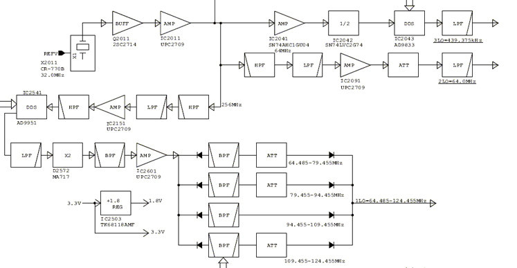 |
Figure 3 is a simplified representation of the DDS LO generation subsystem from the IC-7200 block diagram.
As in the IC-7000, the Analog Devices AD9951 DDS is clocked from a master oscillator/multiplier chain which incorporates an LPF and an HPF, to ensure that the clock signal is as spectrally pure as possible.
The DDS output is a very close approximation to a pure sine wave. The output signal is multiplied up to the required LO frequency range by a frequency doublers. The doubler output is "cleaned up" by a bank of switched BPF's; the appropriate filter is selected for the required frequency range. These filters reduce the noise sidebands generated by the DDS and doubler.
What is interesting about this new LO architecture is that it achieves superior sideband noise performance without the use of phase-locked loops (PLL). The inherent phase jitter of PLL circuits, a significant source of phase noise in conventional synthesisers, has been eliminated in this design.
The combination of the compact, partially relay-switched front end and the "pure DDS" 1st LO, now encountered in the IC-7000, offers excellent dynamic receiver performance in a compact package. It is apparent that the new DDS architecture is being deployed in many new Icom HF and all-mode/multi-band radios. To quote my dear friend George W5YR (SK), "We shall see...."
Text copyright © 2006-2010, A. Farson VA7OJ/AB4OJ. Block diagrams courtesy Icom Inc.
Last updated: 11/15/2012