Problem:
My IC-7800 final MOSFET was blown off during DX QSO last year. The output RF power at that moment was 200W and continuously running for more than 3 hours. I have replaced both faulty final SD-2931. After that, I don't want to operate with full power.
I had another bad experience this year, which is IC-7800 died again, there is no problem in receiving but was not able to transmit. I thought the final went off again and I replaced it, but it was not successful, moreover, driver MOSFET SD-2918 was also replaced, but the problem was still not fixed. All the test points showed that the appropriate voltage indicated in the service manual. was not found any short-circuit problems. So it seemed that the amplifier board was healthy. I can't find any data of the Main unit (J801) RF output power from service manual. I struggled at this point. Is the issue from the Main unit or Power amplifier.?.. how to differentiate?...
I searched through google and found out that two HAM's videos on You-Tube which are Sergio - IK4AUY and Tony - I5NQK. I emailed them and they responded very fast. They suggested me to do some testing. I don't have required test equipment to proceed further, at this moment I realised that it was not possible to proceed any repair work in my QTH.
Saviour:
Singapore HAM's are fortunate because we have Jeff - 9V1AS here. He has all kinds of spectrum analyzers and test equipments. He came to my QTH and understood the situation, then he took the rig along with him. He spent some time rectifying this problem even during his busy projects ongoing.
I have kept the IC-7800 double box for some time, it was too big and occupied more space, so I disposed it. IC-7800 weighed more than 25 kg, If I were to send it to Japan for repairing, shipping cost ....no need to say..!! For this repairing work, I didn't spend any $. What a HAM sprit! Thanks a lot Jeff.
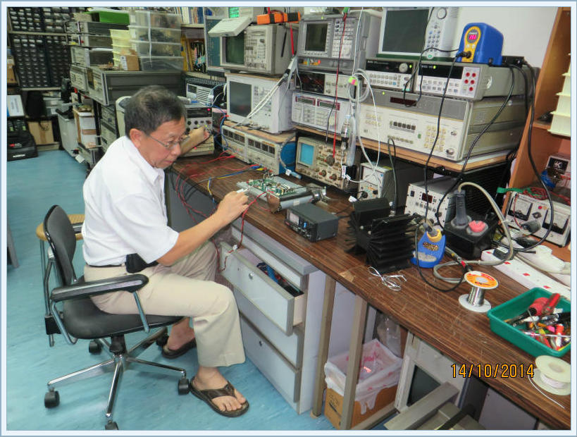
Jeff's test bench
I invited him to write a brief article on what he did to solve this problem because it might help those who suffered the same issue. I extracted the article from his website ( http://jeff9v1as.wordpress.com/2014/11/05/repairing-an-icom-ic7800-power-amplifier/ ) and republished here.
Some time back, I got a call from my good ham friend Siva 9V1SV. He was not his usual happy self. Sad news! His beloved ICOM IC7800 had died – no output. He said that it had happened before, but this time, replacing the MOSFET finals did not help. The next weekend, a few of us went to his QTH. The party, comprising my XYL, Frankie Zuniga 9V1FZ and myself arrived to find the IC7800 lying sadly on the table, dismantled, thick towel beneath, with the power amp module partly tilted up. All of us felt sad. Such an expensive rig, pretty display, good quality knobs, good everything, but no output – not even a teeny weeny flick on the power meter.
Frankie, Siva and myself helped to carry the patient downstairs to my car. HEAVY RIG! Work pressures kept me from working on the repairs too soon. In the meantime, Siva “downgraded” himself to using his spare rig. I spent some time searching the web on the topic of IC7800 PA failures – not much found. Either the PA did not fail much or not many hams could afford the rig. I suspected the latter. Looked like I was pretty much on my own… I downloaded the IC7800 manual and printed out the relevant sections – mainly the PA schematics. It was all conventional looking circuitry, nothing special.
Once the rig was in the shop, with calm mind, the first thing to do was to ascertain that the “no output” was actually due to the PA and not the circuitry driving the PA. This task proved to be easier said than done. The rig used that kind of funny non-standard connector to connect into the RF input of the PA. I have seen that kind of connector when I was refurbishing my old ICOM IC725. In fact ICOM commonly uses this kind of connector to make inter-board RF connections
Here is a picture of that type of connector:
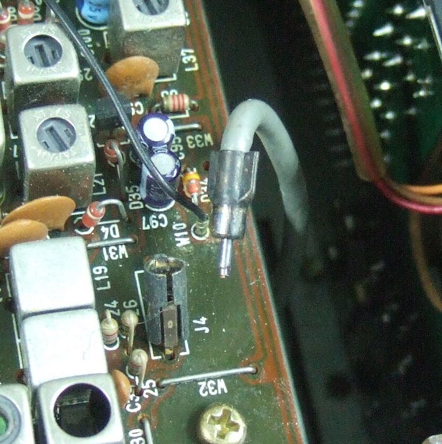
Fig 1. RF connector made of unobtainium
As you can see, there was little chance to make a good RF connection to the PA input from my signal generator. I thought that perhaps it would be better just to see if there is a signal from the stage feeding the PA. I did this by wrapping some wire around the signal pin of the connector and sending the signal into my Anritsu MS2712 spectrum analyzer. I got Siva to tune to 14MHz, AM, and then key the rig via the mic. Sure enough, there was signal. Still, there was still the small chance that although I could see a signal on the SA, it could be too small to drive the PA. Going through the IC7800 manual, I could not find any info on expected signal levels into the PA. Looking at the PA schematics, I noted that there was a Driver, a pre-driver and a pre-pre-driver. This means that we can expect only a small signal into the PA input connector. Subsequent experience (after the repair) proved me correct on this count.
At this point, I was pretty sure that the problem laid within the PA module. Just to gain more insight into the situation, I connected an analog ammeter in the 48V DC line feeding the PA. It read 3A, just as the manual said. Keying the rig made no difference in the ammeter reading. I asked Siva whether he had adjusted the standing current pots, and he said no. He merely replaced the MOSFET finals. Judging from the current, I concluded that the 2 finals and driver MOSFETS are OK (well, at least not OPEN or SHORTED).
I appraised the situation again. Was I going to work on the PA with it connected to the rig? I am not young anymore, and I can’t work with my body BENT OVER the rig (my neck and shoulder strains came back lately). Moreover the rig was too deep for my work bench. If I left it on my workbench, I would not be able to work on anything else, and the repair might take WEEKS – and I had other project datelines to meet. At that point, I decided that it would be best to dismantle the PA module out of the rig and work on it separately on the bench. This proved to be the correct decision, alas with some hurdles, as we shall see later.
The next diagram shows the equipment setup used for the repair. Since the PA module was light and small (about the size of a sheet of A4 paper), it was easy for me to work on this repair in between other projects. I like to work on clean boards, so the first thing I did was to remove the flux residue left by Siva’s replacement of the MOSFET finals. This was carried out using an old toothbrush dipped into flux remover. At least, that removed one area of concern, viz leakage paths.
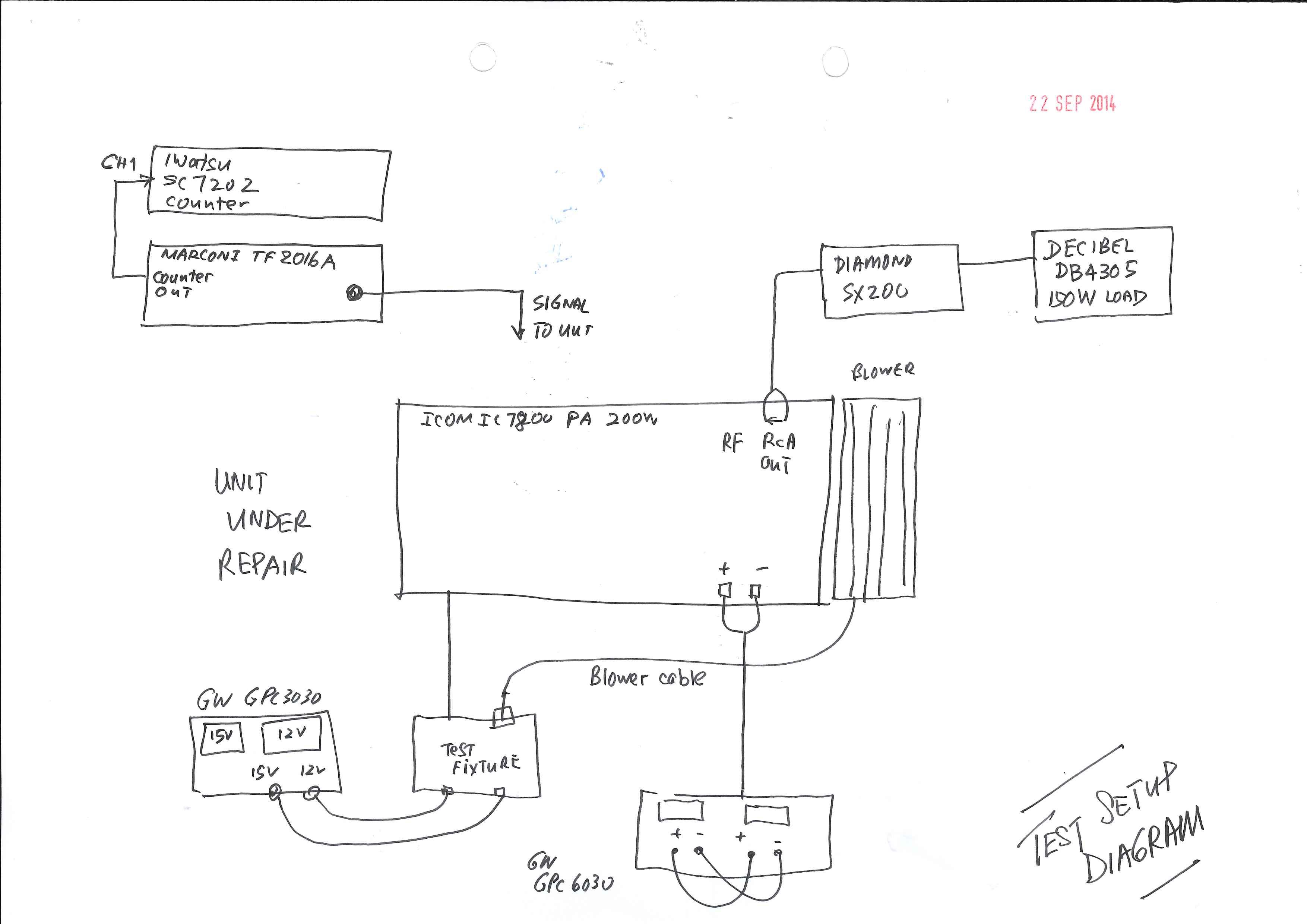
Fig 2. Diagram of the repair setup
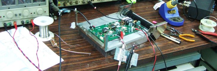
Fig 3. Photo of the repair setup
The signal source I used was my Marconi TF2016A. An internet search reveals that it was built in 1975 (39 years ago). That the switches, especially the attenuator, works is a testimony to how these old equipment were built to last. Being an “old school” analog source, it lacks a digital readout. This was solved by connecting an Iwatsu SC7202 counter to the rear aux RF output of the Marconi. Once warmed up, the frequency hardly drifts, even though it is a pure open loop design. I tend to leave this sig gen on 24/7 and it hardly gives any trouble.
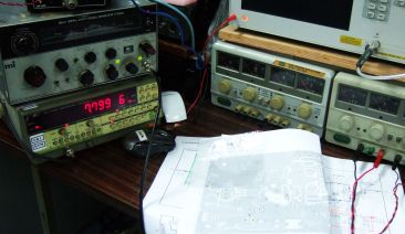
Fig 4. Marconi TF2016A and its “digital readout”
Since the IC7800 has a frequency range extending down to 160m, I figured that a test frequency around 7MHz would be quite suitable for injection. At this relatively low frequency, I would not have to worry too much about standing wave or matching effects, and it would also allow me to probe around the circuit and view the RF signals on an oscilloscope.
Hurdle #1:
The first hurdle was in getting the RF from the sig gen into the board. As mentioned before, the input connector was of a non standard variety.
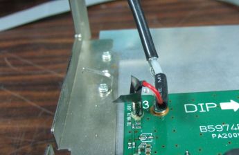
Fig 5. Unsuccessful “roll-your-own” input connector
This photo shows how I tried to “roll my own” connector. It comprised a length of RG58 terminated in a pogo pin. This pin was then inserted into the female connector on the board. Contact was at best intermittent, and I gave up after a while.
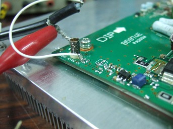
Fig 6. Successful injection into the first stage
This picture shows how I finally managed to inject a signal reliably into the board. I avoided the connector totally, and instead soldered a 0.1uF 0805 size MLCC cap onto the PC track. To the other end of the cap, I connected the center of the RG58 leading to the sig gen. I was to use this same method again to inject signal into the second stage.
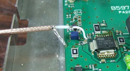
Fig 7. Successful injection into the second stage.
This picture shows how signal was injected into the second stage after removing the interstage coupling capacitor.
Hurdle #2:
The next thing to solve was how to connect the RF output to the power meter and dummy load.
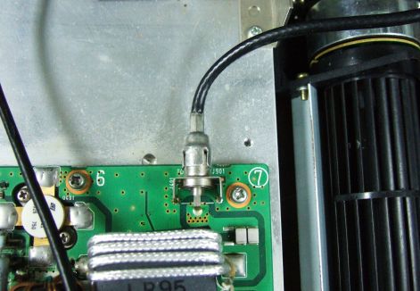
Fig 8. The RF output uses an audio connector!
I was very surprised to find that an “RCA” audio connector was used to carry 200W of RF power. Fortunately, I had some old cables from my audio preamp, and the next photo shows how I pressed it into service using an RCA to BNC adapter followed by a BNC to SO-239 adapter.
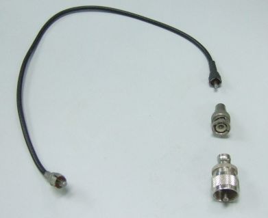
Fig 9. RCA Audio to SO-239 adaptation
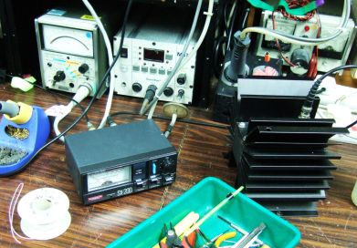
Fig 10. Diamond SX200 and Decibel Engineering DB430S 150W Dummy Load
Hurdle #3:
Now that the PA was out of the rig, there was a need to feed in the various control signals in addition to making the input and output RF connections.
The important signals are the 15V and 48V Supply and the TX Trigger signal. The 15V is used for the first stage, the 48V is for the finals and the TX trigger controls the biasing.
I made a small test fixture for the 15V and TX trigger signals. The 48V was connected direct to the screw type supply input signals. The next few figures show the test fixture is connected into the PA module. Essentially, the 15V and TX trigger signals are soldered directly onto the board, since I did not have the mating connector for J2.
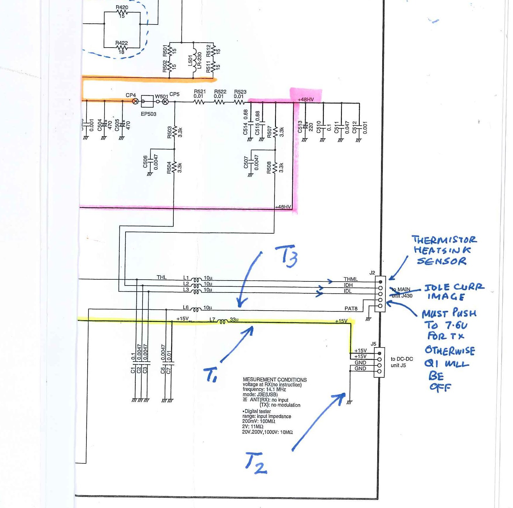
Fig 11. Schematic fragment showing the control inputs which must be fed into the PA module
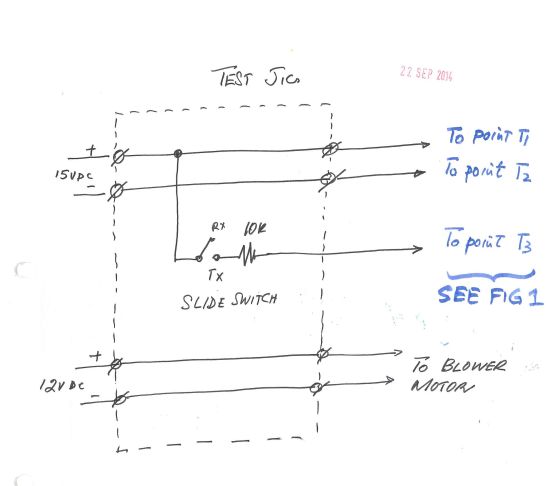
Fig 12. Schematic of the test fixture
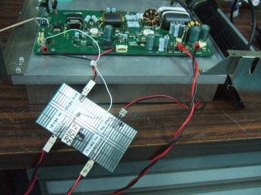
Fig 13. Picture of the test fixture.
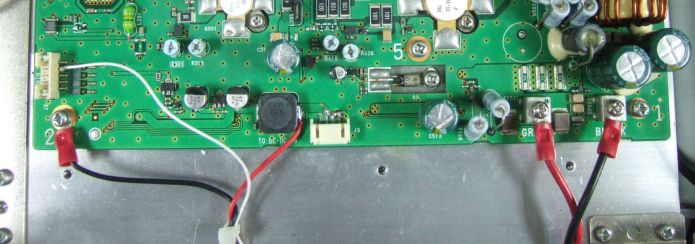
Fig 14. This picture shows how the test fixture is connected into the PA Module
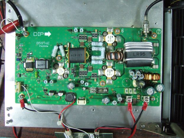
Fig 15. Birds eye view of the repair unit with the RF and test fixture coonections
Troubleshooting and Fault Isolation:
For this section, please refer to Figs 16 and 17 below
.
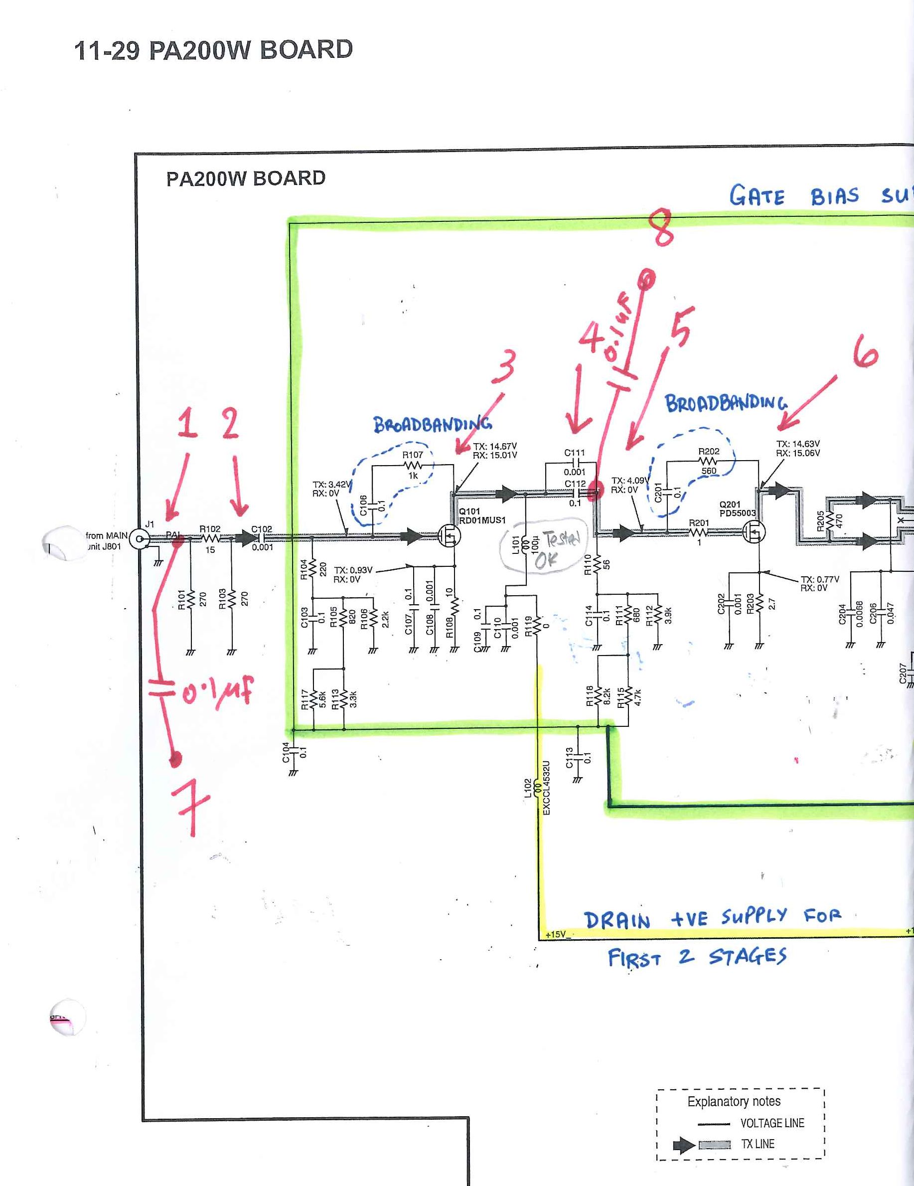
Fig 16. Input Circuit showing various signal injection points
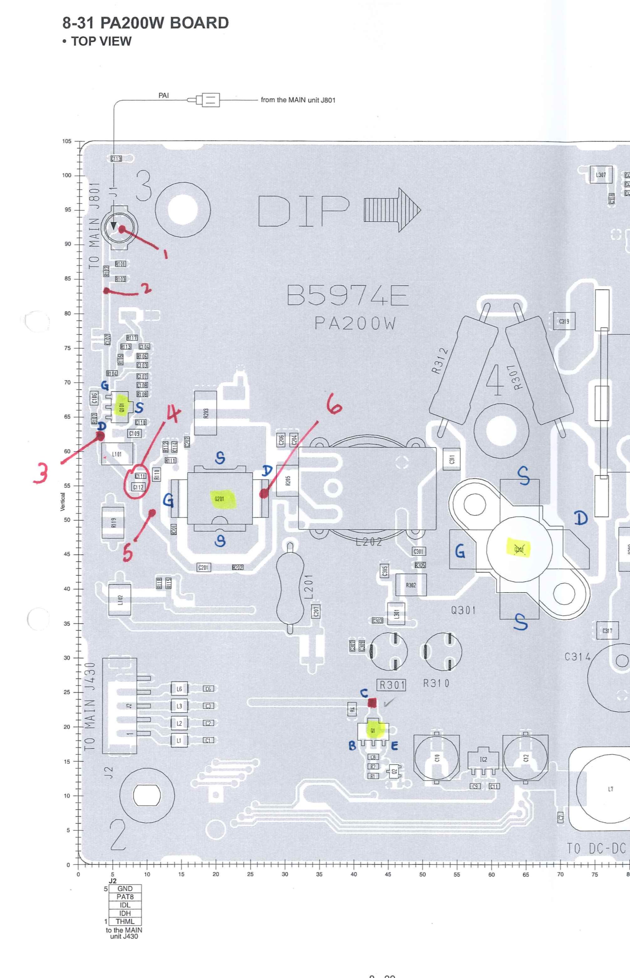
Fig 17. Showing the physical placement of the signal injection points
For the ensuing description, please refer to the schematic of Fig 16, unless otherwise stated. I started troubleshooting first injecting a 7MHz signal into point #7. The 0.1uF SMT cap, as mentioned previously was soldered onto the PCB trace. Using the oscilloscope, I observed the signal at point #1 and also at point #7, after the attenuator comprising R101,R102,R103. The TX / RX is selected by the TX Switch in Fig 12. This is the GREEN line in Fig 16. Placing the probe on the GATE of Q101, it is observed that the DC level drops to 0V in RX and goes positive in TX. Now, setting the scope in AC mode, and cranking up its sensitivity, I could see the 7MHz signal at the GATE. Shifting the probe to the DRAIN of Q101 and setting the mode to TX, I could not see any 7MHz signal. So, Siva had been suspecting the finals, when the problem was actually in the first stage.
In order to vindicate the rest of the PA module, I removed the interstage coupling capacitors #4 (C111,C112) and injected a signal into the second stage Point #5 via a 0.1uF SMT capacitor at Point #8. Setting the switch to TX, the PA started outputting power. Since my 48V PSU could only give a total of 6A, I turned down the output level on the Marconi. This confirmed that the problem laid in the first stage, i.e Q101 or its related components. Q101 was a Toshiba RD01MUS1, but I did not have any. I contemplated replacing it with the 2SK2973 of which I had some, but I decided that it was not a good idea.
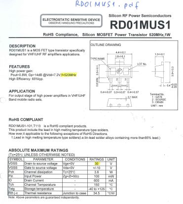
Fig 18. Datasheet for Q101
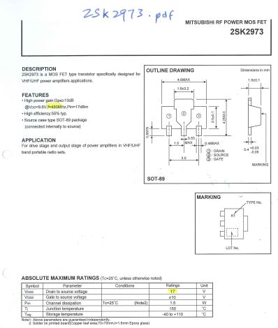
Fig 19. Datasheet for 2SK2973
The datasheets for the 2 transistors are shown in Figs 18 and 19. I decided not to try out the 2SK2973 device due to its lower voltage rating – see the yellow highlights. So Siva had to wait sometime while waiting for the RD01MUS1 to arrive.
When the devices arrived (I had ordered 5 pcs), I got a colleague with better eyesight to replace Q101. Injecting signal at point #7, I could not get anything at point #3. Not a good situation! I concluded that I had possibly thrown out a perfectly good RD01MUS1. Still, the problem must be lurking somewhere in the first stage. I had previously checked the GATE bias circuit levels in TX and RX modes – they were OK. Could L101, the 100uH choke be bad? With all the drain DC current passing through it, there’s a possibility that it could be burnt out. So I desoldered it and tested it on my HP4342 Q Meter. It was OK. So I soldered it back.
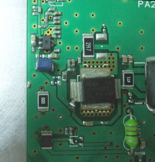
Fig 20. Showing L101 the drain choke for Q101 (blue, left center)
I went home to sleep on the problem. Next day, I decided on a long shot. I suspected that the soldering job on Q101 could be bad, so using a desoldering vacuum sucker, I desoldered it and carefully cleaned the pads. This time I PERSONALLY soldered it. Injecting signal into Point #7, the whole PA came alive – all OK! The standing current adjustment was a non-event.
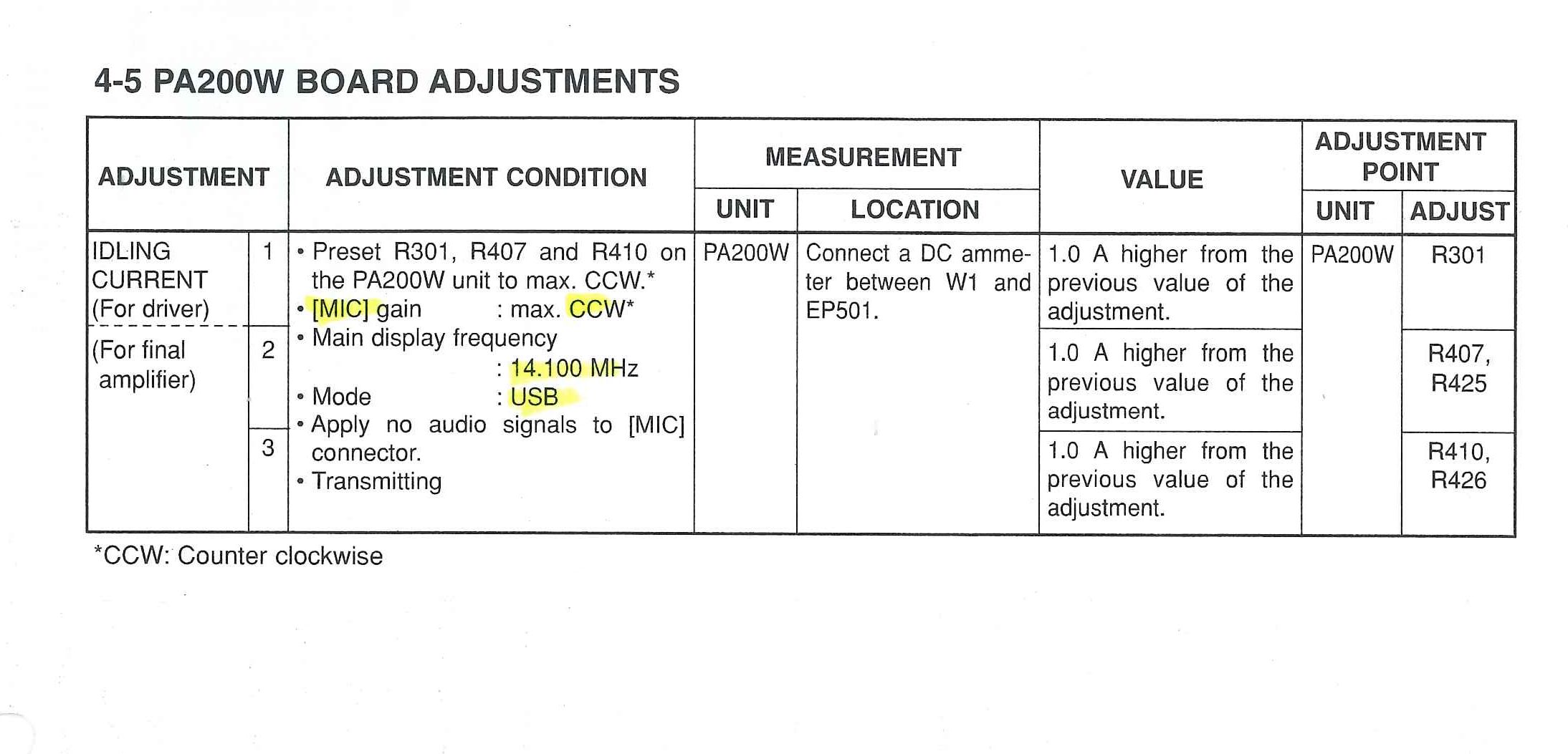
Fig 21. IC7800 Manual on Standing Current Adjustment
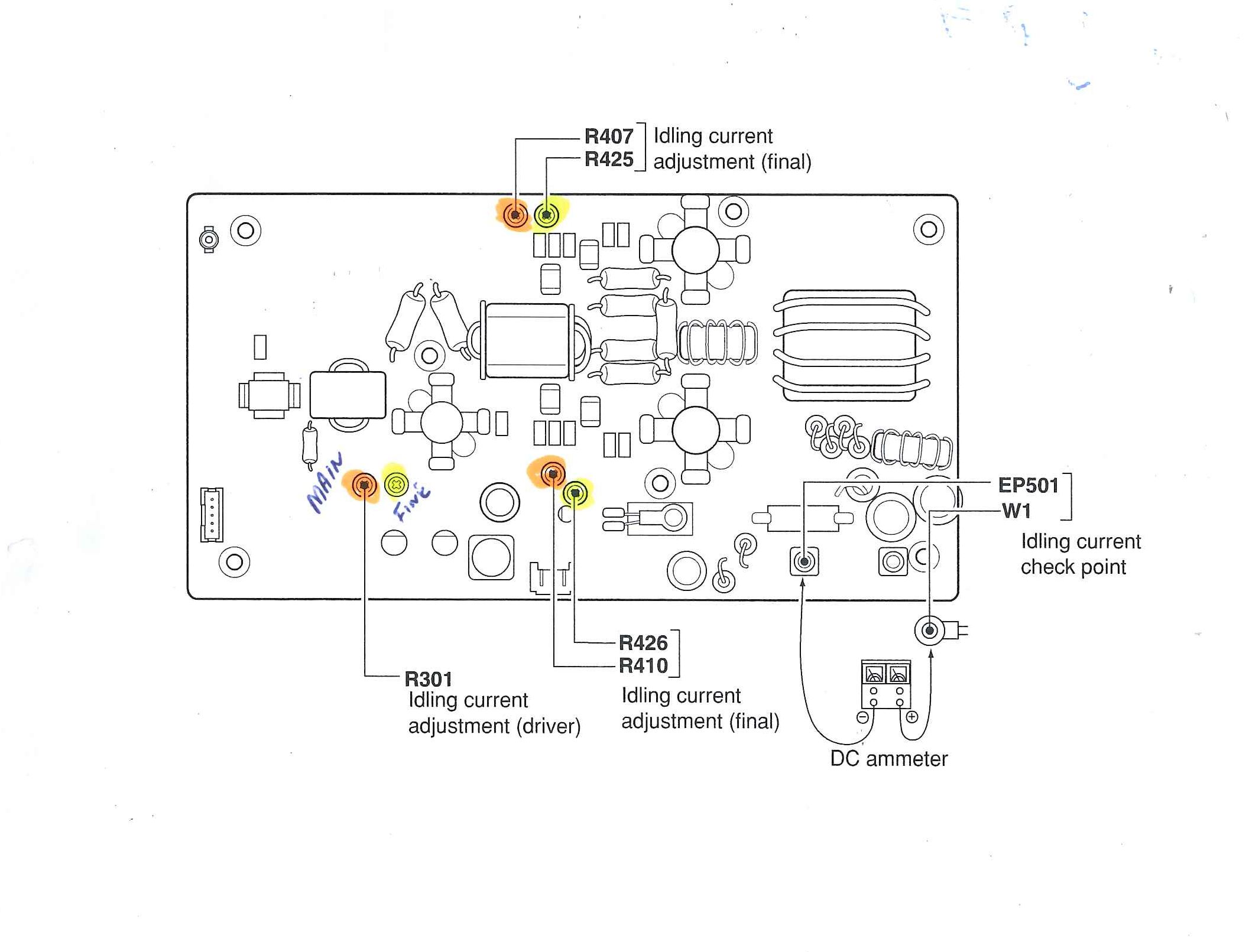
Fig 22. Standing current pots physical locations
The procedure was very straightforward and I adjusted it according to the description in Fig 21.
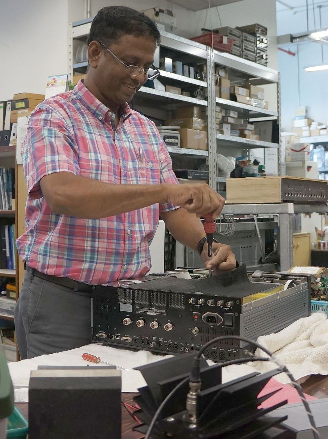
Fig 23. Siva putting back the covers.
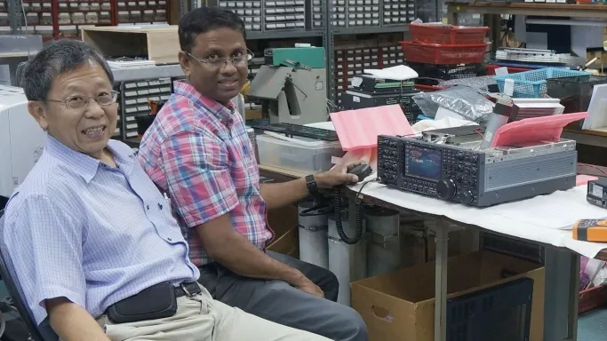
Fig 24. Two Happy Hams!
If you have read up to here, I thank you for your patience.
73
Jeff 9V1AS