Return to Index
Return to Projects
This project was an experiment in reverse engineering the serial control protocol for the AN6311NFA PLL. (found in the Uniden UH036SX UHF transceiver)
The goal was to convert this radio for operation on the 70cm amateur radio band. This was unsuccessful as the VCO will not oscillate at the right frequencies for 70cm operation (the VCO control voltage bottoms out before the VCO gets anywhere near the 70cm band). The VCO is too small and it is too hard for me to trace the multilayer board tracks (I do not have a service manual for this radio) so I can not change the frequency determining components of the VCO. Please note that the antenna was removed from this radio and replaced with a dummy load for these experiments.
However, all is not lost. This project was a valuable learning experience and with any luck, the tools that I produced in the process (essentially a crude logic analyser) will be able to be used to reverse engineer other serial PLL control protocols.
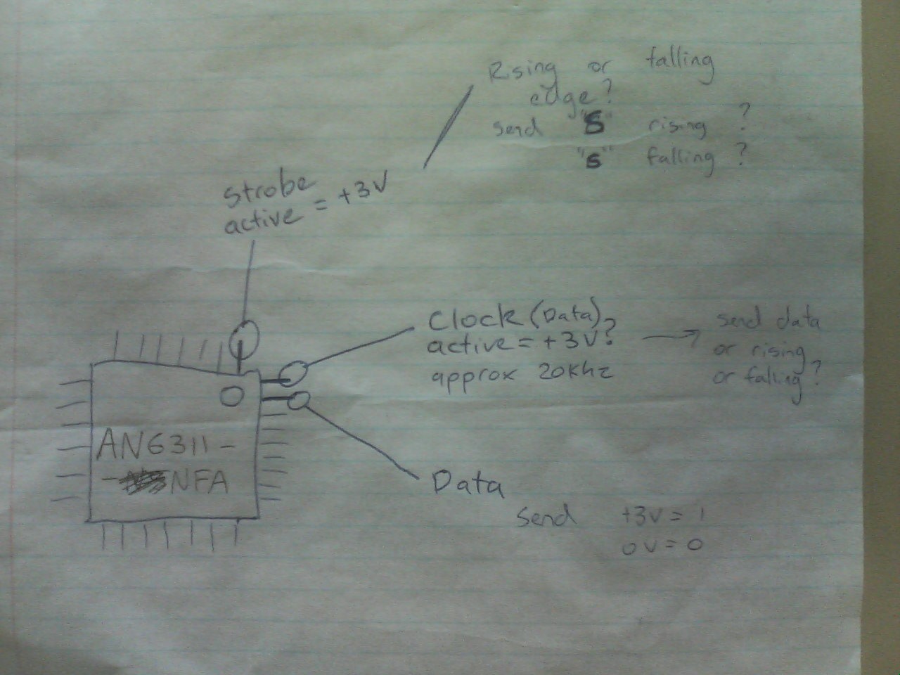
I was unable to find a datasheet for the AN6311NFA, however, I was able to find data on two similar ICs made by the same manufacturer. This, combined with my oscilloscope, allowed me to identify the serial control lines on the AN6311NFA.
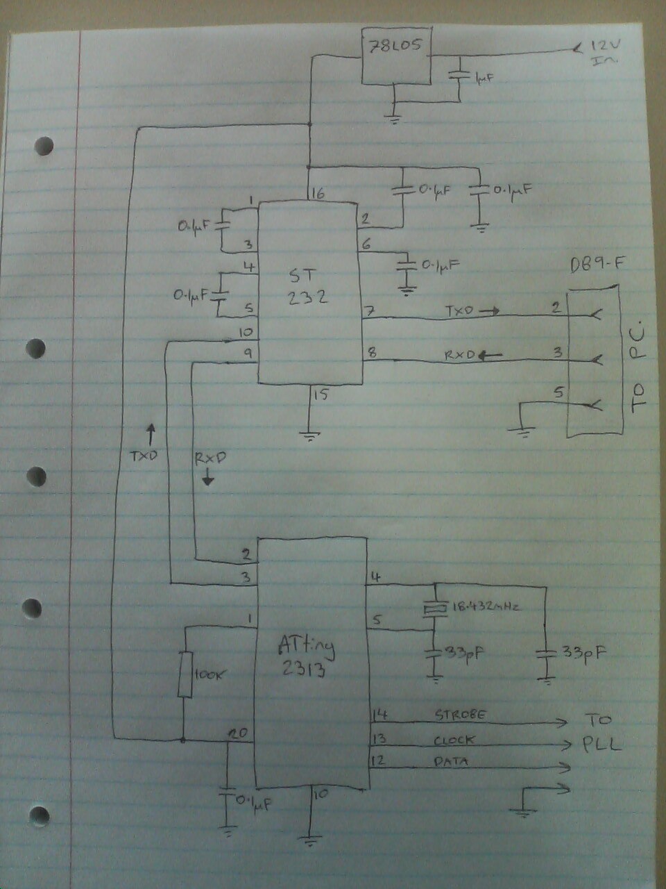
One board with an ATtiny2313 microcontroller (clocked at 18.432 Mhz) and an ST232 RS232<->TTL level converter was constructed. One complication encountered was that the PLL was supplied from a 3.3V DC power supply, when spying on the serial comms to the PLL this is not a problem as 3.3V is enough voltage to register as a logic high on the tiny2313's input pins (when the tiny2313 is supplied with 5v). However, when driving the PLL, care must be taken to limit the voltage on the PLL input pins to 3.3V or less, I did this by using pullups between the PLL input pins and the radio's 3.3V rail and by using the tiny2313's outputs to pull the PLL input pins low when a logic 0 was required.
Three different firmware programs were written, two which spy on the PLL serial control and dumps the data out an RS232 port for logging on a PC, and the other which receives commands from a PC on an RS232 port and then outputs those commands to the PLL.
Spying on the PLL serial comms - pllsnoop
Pins 12, 13 and 14 on the ATtiny2313 are used as input pins to monitor communications to the PLL.
The first firmware (which didn't work as desired), sent different ASCII serial characters to the PC when a state change on an input was detected (c = clock low, C = clock high, s = strobe low, S = strobe high, 0 = data low, 1 = data high). It was however, sufficient for me to establish which bits control the PLL frequency and the NBIF RX portion of the PLL IC.
The second firmware polls the input pins for a state change, and when a state change is detected, the binary states of all these inputs are converted into an ASCII character which is stuffed into the serial transmit buffer. This ASCII character is from 0 to 7 inclusive, and is determined as follows:
char = 0
if (pin 12 = high) then char += 1 ;data line
if (pin 13 = high) then char += 2 ;clock line
if (pin 14 = high) then char += 4 ;strobe line
send char to serial port
The serial transmit routine sends ASCII characters from the buffer to the PC at 115,200 bps. PLL commands received on the PC look like this:
1020131020201310201310202013131310202020131020201326401
which can be translated to:
1000111000001110001110000011111110000000111000001100001 data
0010010010100100100100101001010100101010010010100111000 clock
0000000000000000000000000000000000000000000000000001100 strobe
It appears that data is clocked into the PLL on the rising edge of the clock, and strobed into the register on the falling edge of the clock when strobe is high.
Decoding the PLL command structure
(in the below listings, 0s and 1s represent data and S the strobe)
When the radio is powered on with it's power button, the following commands are sent to the PLL:
S1s reset the PLL or just a glitch?
0101110001000000101S cmd: turn on RX
0000000110010100111S cmd: Frequency follows
0100111000100000001S Frequency: 499.75Mhz - why tune this frequency on startup?
0101110001000000101S cmd: turn on RX
0101110001000000101S cmd: turn on RX
0000000110010100111S cmd: Frequency follows
0100100011001011001S Frequency: chan#1 PRS rx
delay approx 0.1sec
0101111001000001101S cmd: sleep
delay approx 0.9sec
0101110001000000101S cmd: turn on RX
0000000110010100111S cmd: Frequency follows
0100100011001011001S Frequency: chan#1 PRS rx
delay approx 0.1sec
0101111001000001101S cmd: sleep
delay approx 0.9sec
0101110001000000101S cmd: turn on RX
0000000110010100111S cmd: Frequency follows
0100100011001011001S Frequency: chan#1 PRS rx
delay approx 0.1sec
0101111001000001101S cmd: sleep
...continues...
From this we can see that the radio is operating in a power saving mode when the squelch is closed - the PLL and NBIF RX is only powered up for about 1/10second every second. These commands were figured out by probing the radio's circuitry with an oscilloscope, and comparing the commands to the sate of the radio.
When the radio is powered off with it's power button, the following commands are sent to the PLL:
...
delay approx 0.9sec
0101110001000000101S cmd: turn on RX
0000000110010100111S cmd: Frequency follows
0100100011001011001S Frequency: chan#1 PRS rx
delay approx 0.1sec
0101111001000001101S cmd: sleep
delay approx 0.9sec
0101110001000000101S cmd: turn on RX
0000000110010100111S cmd: Frequency follows
0100100011001011001S Frequency: chan#1 PRS rx
0101110001000000101S cmd: turn on RX
0101111001000001101S cmd: sleep
no further commands
When the radio is powered on and PTT is pressed, the following commands are sent to the PLL:
0001110001000000101S cmd: turn on TX (probably mutes NBIF RX)
0000000110010100111S cmd: Frequency follows
0100101001110001001S Frequency: chan#1 PRS tx
Whent PTT is released, the following commands are sent to the PLL:
0101110001000000101S cmd: turn on RX
0000000110010100111S cmd: Frequency follows
0100100011001011001S Frequency: chan#1 PRS rx
delay approx 0.1sec
0101111001000001101S cmd: sleep
delay approx 0.9sec
0101110001000000101S cmd: turn on RX
0000000110010100111S cmd: Frequency follows
0100100011001011001S Frequency: chan#1 PRS rx
delay approx 0.1sec
0101111001000001101S cmd: sleep
...continues...
When the channel step button is pressed, the following commands are sent to the PLL:
0101110001000000101S cmd: turn on RX
0000000110010100111S cmd: Frequency follows
0100100011001011001S Frequency: chan#1 PRS rx
push chan up button
0101110001000000101S cmd: turn on RX
0000000110010100111S cmd: Frequency follows
0100100011001100001S Frequency: chan#2 PRS rx
Scanning is same command pattern as manual channel change. If manually changing channels with squelch closed, cmd: sleep will be sent to the PLL a short time after channel change if the squelch remains closed.
Decoding the frequency command
Chan Frequency control (19 bits)
RX01 010 0100 0110 0101 1001 = 149,081
RX02 010 0100 0110 0110 0001 = 149,089
RX03 010 0100 0110 0110 1001 = 149,097
RX39 010 0100 0111 1000 1001 = 149,385
RX40 010 0100 0111 1001 0001 = 149,393
TX01 010 0101 0011 1000 1001 = 152,457
TX02 010 0101 0011 1001 0001 = 152,465
TX03 010 0101 0011 1001 1001 = 152,473
Adjacent PRS channels are 25Khz apart, and from the above, the PLL divisor (frequency control data) varies by 8 between adjacent channels. This tells me that the PLL reference is 3.125Khz (25Khz/8). This also agrees with the presence of the 8Mhz PLL clock crystal (8MHz/2560 = 3.125KHz).
The difference between the PLL divisors for RX and TX on the same channel is 3376, which is equivalent to 10.55 MHz (3376 * 3.125KHz) - this agrees with the hardware as the 1st IF ceramic filter in the radio is marked 10.5MHz.
For example, PRS channel #1 is 476.425MHz and 152,457x3.125Khz is 476.428Mhz - this discrepancy is likely to be due to a slight frequency error in the PLL reference clock (eg 476.425Mhz/152,457 = 3.1249795 KHz instead of the nominal 3.125Khz).
So, with the control formula of divisor = frequency/3.1249795 KHz, we can generate frequency control commands for the 70cm band:
TX 432.500Mhz/3.1249795Khz = 138,401
RX 443.05MHz/3.1249795Khz = 141,777 (432.500Mhz RX frequency + 10.55Mhz 1st IF = 443.05MHz LO)
Sending commands to the PLL - pllprog
The OEM microcontroller was removed from the radio and pins 12, 13 and 14 on the ATtiny2313 were used as output pins to send commands to the PLL.
This firmware receives ASCII characters from the PC on the mcu serial port at 115,200bps and changes the state of the output pins depending on the state of the ASCII characters. The ASCII character format is very similar to that used for the first attempt at monitoring the serial PLL commands (c = clock low, C = clock high, s = strobe low, S = strobe high, d = data low, D = data high).
To send a command to the PLL, both strobe and clock need to be pulled low, then the first bit of data can be set on the wire, and clock is then pulsed high to latch the data into the PLL, then the next bit of data is set on the wire, and the clock is pulsed high again, an so on, until the after the rising edge of the clock for bit 19, when the data line is cleared, strobe set high, clock pulled low and finally strobe pulled low.
For example, to activate the receiver and tune PRS channel #1:
...0..1..0..1..1..1..0..0..0..1..0..0..0..0..0..0..1..0..1.Strobe - cmd: turn on RX
scdCcDCcdCcDCcDCcDCcdCcdCcdCcDCcdCcdCcdCcdCcdCcdCcDCcdCcDCdScs
...0..0..0..0..0..0..0..1..1..0..0..1..0..1..0..0..1..1..1.Strobe - cmd: frequency follows
scdCcdCcdCcdCcdCcdCcdCcDCcDCcdCcdCcDCcdCcDCcdCcdCcDCcDCcDCdScs
...0..1..0..0..1..1..1..0..0..0..1..0..0..0..0..0..0..0..1.Strobe - frequency: 499.75Mhz
scdCcDCcdCcdCcDCcDCcDCcdCcdCcdCcDCcdCcdCcdCcdCcdCcdCcdCcDCdScs
...0..1..0..1..1..1..0..0..0..1..0..0..0..0..0..0..1..0..1.Strobe - cmd: turn on RX
scdCcDCcdCcDCcDCcDCcdCcdCcdCcDCcdCcdCcdCcdCcdCcdCcDCcdCcDCdScs
...0..1..0..1..1..1..0..0..0..1..0..0..0..0..0..0..1..0..1.Strobe - cmd: turn on RX
scdCcDCcdCcDCcDCcDCcdCcdCcdCcDCcdCcdCcdCcdCcdCcdCcDCcdCcDCdScs
...0..0..0..0..0..0..0..1..1..0..0..1..0..1..0..0..1..1..1.Strobe - cmd: frequency follows
scdCcdCcdCcdCcdCcdCcdCcDCcDCcdCcdCcDCcdCcDCcdCcdCcDCcDCcDCdScs
...0..1..0..0..1..0..0..0..1..1..0..0..1..0..1..1..0..0..1.Strobe - frequency: chan#1 PRS RX (465.875Mhz LO -> 476.425Mhz RX)
scdCcDCcdCcdCcDCcdCcdCcdCcDCcDCcdCcdCcDCcdCcDCcDCcdCcdCcDCdScs
To sleep the receiver:
...0..1..0..1..1..1..1..0..0..1..0..0..0..0..0..1..1..0..1.Strobe - cmd: Sleep
scdCcDCcdCcDCcDCcDCcDCcdCcdCcDCcdCcdCcdCcdCcdCcDCcDCcdCcDCdScs
To TX on PRS channel #1:
...0..0..0..1..1..1..0..0..0..1..0..0..0..0..0..0..1..0..1.Strobe - cmd: turn on TX
scdCcdCcdCcDCcDCcDCcdCcdCcdCcDCcdCcdCcdCcdCcdCcdCcDCcdCcDCdScs
...0..0..0..0..0..0..0..1..1..0..0..1..0..1..0..0..1..1..1.Strobe - cmd: Frequency follows
scdCcdCcdCcdCcdCcdCcdCcDCcDCcdCcdCcDCcdCcDCcdCcdCcDCcDCcDCdScs
...0..1..0..0..1..0..1..0..0..1..1..1..0..0..0..1..0..0..1.Strobe - frequency: chan#1 PRS TX (476.425MHz)
scdCcDCcdCcdCcDCcdCcDCcdCcdCcDCcDCcDCcdCcdCcdCcDCcdCcdCcDCdScs
Testing with the above commands was successful, provided that the frequency command (PLL divisor) was within the range of the VCO.
pllsnoop - assembler source code (please note that this code is defective - use pllsnoop2 instead)
Circuit schematic
ATtiny2313 datasheet
pllsnoop2 - assembler source code
pllsnoop2 - assembled firmware
pllprog - assembler source code
pllprog - assembled firmware
ATtiny2313 assembler include file
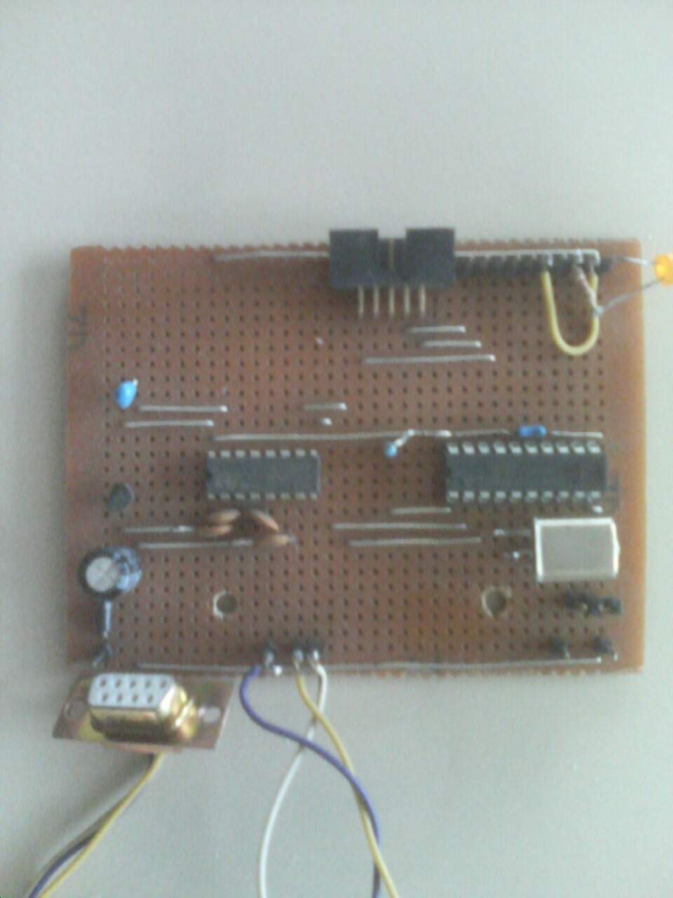
Photo of prototype board
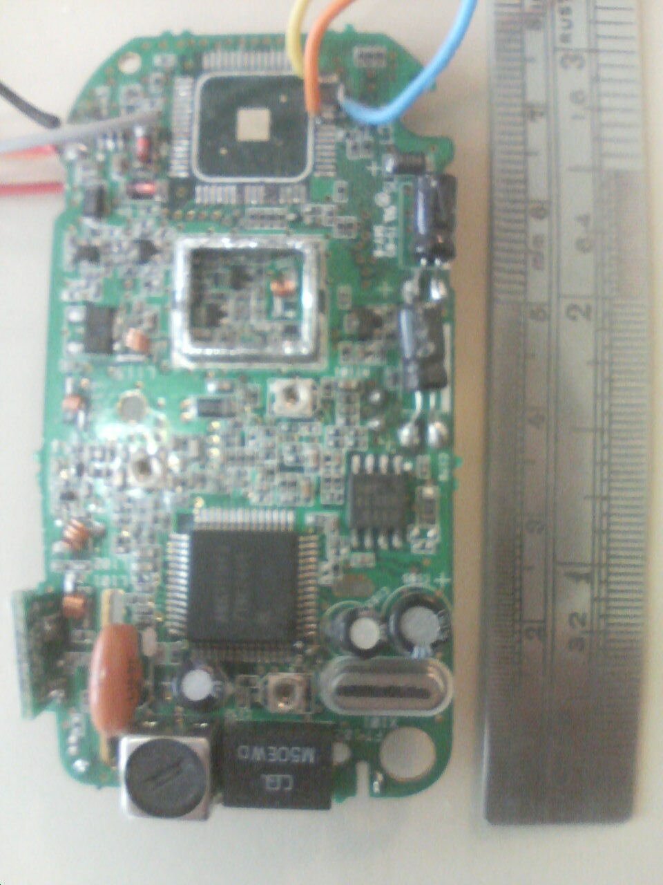
Photo of UH036SX PCB
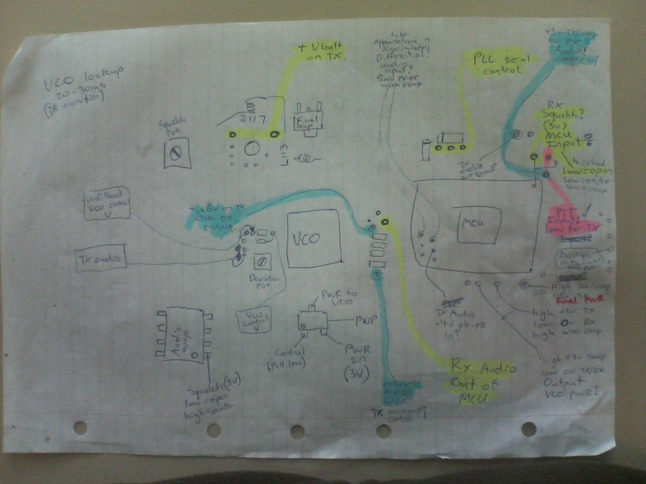
UH036SX notes
AN6311NFA serial pins
Sorry, but no PCB is available for this project.
ST232 datasheet
AN8953NFA datasheet
AN6951BFJM datasheet
This page last updated 4th October 2009