Follow the Micro Core Schematic as you read this description.
Power Supply
The unit is powered by +5V at 20mA (40mA more for PLED display, and up to 400mA when a back-lit LCD display is used). There is a -5V 10mA supply used for
the RS232 interface and perhaps for OCXO ECF bias adjustment, but it is not used by the micro. The power supplies are entirely conventional
and are not described (use 78L05 and 79L05 regulators). Both supplies need to be well regulated and noise-free. Use decoupling
resistors and electrolytic capacitors at the power supply output. Oven power and heater requirements will depend on the oscillator
used, and will not be described, although the oscillator supply should be very noise free and stable - an LM723 regulator
is recommended. Because of the oven heater requirements, battery backup isn't practical, so the unit is best run
from an AC supply with UPS backup. If battery operation is planned, start with a 24V SLA at about 20AH. The oven heater will be
the main load.
Reset Circuit
U1 is the supply monitor and reset device. When the supply is below the upper limit (typically 4.5V), the /RST
output is kept low. This ensures that a clean reset occurs at power-up, irrespective of the power supply rise-time.
The Dallas DS1233 or Motorola MC34064 devices are suitable. The /RST output is open collector, so the output
is pulled up by R21, and the RC time constant R21/C3 defines the reset delay. Other devices (for example the programmer)
can also pull /RST low to initiate reset.
Micro Controller
The brains of the unit is the micro U2, an ATMEL ATTINY2313 or (now obsolete) AT90S2313. This device is a high speed
processor capable of executing up to 10 million instructions/second (10 MIPS) at a 10MHz clock frequency. The device
is clocked by the reference oscillator. If the rise-time of the 10MHz oscillator output is insufficient, or the output
level too low, the micro will need a clock buffer. The rise-time and fall-time should be faster than 1us, and the clock signal
needs to be 0 - 5V (CMOS levels). It is worth using a buffer anyway, to reduce the risk of the micro modulating the reference
(it has been known!) Any other outputs from the 10MHz oscillator need to be separately buffered (not shown here).

The micro has 17 input and output pins, 128 bytes of RAM, a UART and two timers, one with an input capture feature, which
is used in this design to sample the counter at the GPS second event.
In this application most of the pins are outputs, with inputs for serial receive, 1PPS from the GPS and the HOLD input.
Since these latter two signals go off the board to another device, the inputs have protection circuits to prevent
electrostatic damage.
Signal lines without ESD protection are connected elsewhere in the schematic. See the other drawings listed at the bottom
of the main page.

Inside view of the prototype
Click on image to view full size.
While the unit could be much smaller, the prototype was (mostly for convenience) built in the case of an old HP 5326A
Frequency Counter. While much of the circuitry still remains inside,
not much of it used. The HP 10811A reference oscillator (box slightly right of centre) is of course used, along with the
reference buffer/driver board (far right) and the back panel connections. The power supply is used intact, but with the high
voltage (Nixie supply) disabled. The original mother board is used, but was adapted slightly to give access to the EFC pin
of the reference oscillator.
All the added circuitry is on a platform of plain single-sided circuit board, fitted with a right-angle section into the
socket which originally held the display section, where it picks up
+5V and -5V power and ground. The three units are (left to right) the Navman Jupiter-T GPS engine, the GPS Monitor/Display
micro and the VNGBOX micro. The displays are stuck to the inside of the original front panel display filter (grey)
using double-sided tape. (The photos were taken through this filter). The RS232 connectors are at the rear, behind the power transformer, and the GPS antenna cable connects through a ventilation hole on the left side.
Display
The DISPLAY connector is a standard 14 pin dual row boxed header for a ribbon cable to the display. The LCD/PLED display
is operated in 4-bit mode to minimize the number of micro controller pins used.
The micro drives the LCD or PLED display in 4-bit mode. The /WR line of the display is held low,
as the micro never reads from the display. The display is updated regularly every second. The trimpot R5 adjusts the LCD
contrast (typically 1.5V) or the PLED brightness (typically 3V). With LCD, a board-mount trimmer is appropriate, as it will
rarely require adjustment. PLED displays can lose brightness or become uneven if over-used, so a front panel control can be used to turn down
the brightness when the display isn't needed.
Programming
The other connector is the programming header, and is not used after initial commissioning.
The micro is programmed in circuit, with everything else connected. While other circuitry connects to the same pins,
programming is not affected. Some parameters are stored in EEPROM, so the user can change the operating baud rate
and the nominal operating reference frequency to suit the reference used.
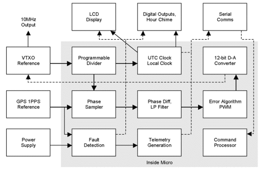
Control system block diagram
Click on image to view full size.
Enlarge the above picture to follow how the unit works.
2kHz Interrupt
The micro controller operates in snooze mode. The main 16-bit timer in the micro hardware divides down from the OCXO
(shown in the diagram as a VTXO) reference frequency, nominally 10MHz, and generates an interrupt to wake up the micro
briefly every 500µsec. At this point the 1 kHz output is toggled and a divide by 2000 software counter stepped.
At this time the Pulse Width Modulators controlling feedback are also cycled. One PWM uses the upper six bits of the 12-bit control value, and the other PWM uses the lower six bits. These synchronous PWM outputs are combined in a 64:1 resistor network to achieve a highly linear yet very simple 12 bit D-A converter.
Once every second the �2000 counter overflows, the 1 sec output is pulsed, UTC time is incremented, and
the output updated. This counter is also synchronized by the GPS 1PPS signal when present, so that the clock runs in time with the GPS. The �2000 counter divides first by 10 then by 200 to give a 5ms timer which controls the time code mechanism.
When each task is done, the processor goes back to sleep. The processor is
very fast, and achieves these tasks very quickly. Thus the average current drawn by the device is
moderately low, despite the high clock speed. Time is kept by the internal clock rather than
GPS, in order to maintain time when GPS is not available.
GPS 1PPS Event
When the GPS 1PPS tick arrives (every second of course), hardware in the micro samples the oscillator phase
from the main timer within the micro. No software is involved, so there is no jitter, and sampling
resolution is 100ns. A 64 second deep 16 bit sample buffer operates every two seconds, and provides an
effective resolution of about 1.5ns, as phase difference is measured across 64 seconds, yet
with (in differential / integral and PID modes) a new solution available every two seconds.
It is this deep buffer and integrating algorithm which provide
high performance without requiring complex hardware circuitry (such as a very high frequency
interpolation oscillator, the normal technique used). When no GPS is available,
no timer sample occurs and the control algorithm freezes. If the GPS 1PPS is
suspect because the fix is poor, an external HOLD command can force the error feedback
to hold, so although poor samples will be made and stored in the buffer, they will not
influence the control algorithm (provided HOLD is not removed until at least 64 seconds
after the GPS 1PPS pulses come right again). The firmware includes a settable timer
(the default integrating period) which is used to allow inaccurate samples to flush
once the HOLD is removed.

The display indicating HOLD mode
Control Algorithms
Thre types of algorithm are provided. These are direct high gain proportional, differential / integral, and proportional and differential / integral (PID).
Mode 0 Differential / Integral
Very good control is achieved using an integrating controller, which can have very high gain, and yet have great stability.
The 64 second differential phase measurement made from each end of the sample buffer is a measure of frequency offset,
with an effective resolution of 0.015Hz (1.56ns). The control algorithm decrements or increments the control voltage
(integrating the error) to keep the differential phase measurement across 64 seconds, and thus the frequency offset
at zero (with a resolution of 1.5 x 10⁻¹²). The rate at
which corrections are added (the integration rate) sets the system software gain. All calculations are made in 16-bit
signed integer arithmetic. The actual phase of the controlled oscillator in integrating mode is arbitrary, but
remains fairly stable for weeks or months on end, and is unaffected by gain change. With high quality oscillators,
some slight offset may be noted (about 1 x 10-12). The reason for this is unclear, but may be a statistical sampling effect.
Because of its good control and fast settling time, this mode (at highest gain) is used as the default mode.
Mode 1 Proportional + Differential / Integral
This mode provides the most accurate control, but has some limitations. Set correctly, it can keep the oscillator within 20ns
of the set point forever.
PID control using integer maths is very difficult to achieve, and even more difficult to make stable! In this implementation,
the differential term is the same as in Mode 0 (across 64 sec, same gain). The proportional term is achieved by finding the
difference between the current phase and an arbitrary but fixed value of xx80HEX, and dividing this difference by four. In order to
prevent loss of resolution, the difference is dithered by �2 before division.
The two terms are then integrated (added) to the error
term. The rate at which corrections are added (the integration rate) sets the system software gain. All calculations are made in 16-bit
signed integer arithmetic. Once locked and stable, the oscillator always sits with a phase value close to xx80HEX. Since the phase
range is from 0 - 4999 (0 - 1387HEX), there are many valid lock points - 0080, 0180, 0280 etc. This makes the time to lock quicker.
This mode takes twice as long to lock (up to 20 minutes) since the differential term must settle before the proportional term winds in,
and the differential term tends to fight the proportional term. The differential term is used to keep the loop stable, since the phase
lag in the low pass filters can make a proportional control system unstable.
A feature to note is that in this mode the phase plot on the PC display will always be right down the middle of the graph (hence the choice
of xx80HEX as the lock points). This is the preferred mode, if your reference is good enough and the mode proves to be stable
in your setup.
Mode 2 Direct Proportional
The high gain proportional control can achieve very fast
lock, and with nominally constant phase. The operating phase wanders about with time, as
a proportional control technique must run in error to produce control. The
resolution is only 100ns, and a new solution is available every second. One advantage of the proportional
controller is that it operates (short term) at a constant phase angle. The phase angle will drift as the crystal
in the reference ages, or if the mechanical adjustment is changed, and also (see the graph below) changes with
gain setting. This high gain mode will lock the
reference in a matter of 30 seconds or so - as fast as the hardware low pass filter will allow. In this
mode, 'n' (see below) sets the rate at which the error is calculated, but does not affect gain.
- In summary, the control modes are:
- Cn0 Differential / Integral (gain ~ 1/n)
- Cn1 Proportional + Differential / Integral (gain ~ 1/n)
- Cn2 High gain proportional (gain = 72)
Hint:
To operate in integrating mode at a fixed phase angle, first operate for 15 minutes or so in mode C02, then switch
to integrating mode - the phase will stay constant (as in the example below).

Illustrating performance in different modes
In the above picture, the phase (green) indicates the long term accuracy of control for each mode. The electrical gain of the
feedback system was temporarily reduced to make the errors more obvious. The EFC feedback voltage
(purple) is a good indication of the amount of noise and frequency error that results. Mode C01 is the PID
mode. Mode C02 hs the high gain proportional mode (gain=72). To the right, integrating mode
C00 (2 sec integration) shows lower noise, but less accurate long term phase control, while finally mode C40
(10 sec integration) shows the lowest noise, but the least accurate long term phase accuracy. Even so, the
phase errors equate to a p-p variance of only 1 part in 109 per hour, even with gain reduced. Better control than
that illustrated is achieved if higher electrical gain is used (between D-A converter and oscillator EFC input) or if the
oscillator has high control range.

Long term control performance
Click on image to view full size.
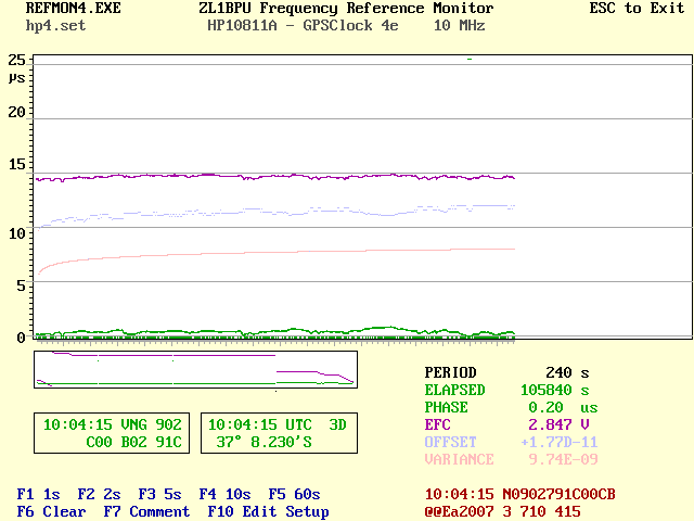
This image shows the ability of the control algorithm (even on the fastest, most noisy integrating setting C00),
integrating over two seconds, to achieve
tight, low noise control. The oscillator is an HP 10811A (10MHz), operating in the VNGBox
prototype. The recording is for just over 29 hours and shows an accumulated p-p variance of 9.74 parts
in 109 (it's actually root variance or deviation). The offset from the nominal frequency should be almost zero. The green trace at the bottom is the oscillator phase, while the purple trace is the EFC
voltage.

10s Tau variance plot
In this picture you see a spreadsheet plot of the oscillator deviation, measured with Tau = 10 (10 second sample rate) in mode C40.
The deviation would seem to be about 5 x 10-11, or about one order worse than the oscillator free-running
specification (5 x 10-12). Not bad performance, given that the time resolution of the VNGBox unit without software
tricks is only 100ns! The data was recorded
using an HP 5315A frequency counter in time interval average mode, comparing with an HP 5065A Rubidium reference
(AV 1.6 x 10⁻¹² at 10 sec Tau). The data was recorded manually, and massaged with a 1/50Hz high pass filter to remove Rubidium
Standard offset without affecting the variance.
Subsequent independent measurement of variance using a Pendulum CNT-90 counter and HP E1938A free-running
high stability reference confirmed Allan Deviation (Root Allan Variance) below 1.0 x 10⁻¹¹ for
Tau 0.2 to 20s. Beyond 20s Tau the Allan Deviation degraded due to limited VNGBox D-A converter resolution. Measurement
system limitations prevented measurement at shorter time intervals. See the graph below:

VNGBox Independent Allan Deviation results
Local Time Clock
Time is kept in Packed BCD format (Binary Coded Decimal), where the lower four bits
represent the units 0 - 9, and the upper four bits
represent the tens. This makes counting more tricky, but simplifies display. Every time the
UTC time is incremented, the BCD values need to be checked to ensure they follow the BCD format,
which means checking that the low nibble is <10 and the high nibble <6. The hour is checked to see
that it remains <24, and is set to zero when 23 is exceeded.
Local time can be set ahead or behind UTC, in one second increments, so can represent any time zone. Further, because the time
transmitted by a time code represents the time of the following minute, the time should be set one minute in
advance of UTC (or whatever time standard used) for time code transmission. The time code is discussed elsewhere.
The date is not kept, and leap seconds must be added manually (push the '-' key on the PC).