Detailed Description
-
Southern Avionics SC1000 DGPS USCG Dual Transmitter
Introduction
This is a detailed description only of the Transmitter Unit, Antenna Tuner, and as much of the rest of the system as is needed to understand operation in detail.
The Charger, RSIM Unit and Inverter are not covered. Those interested in building an LF transmitter of reasonable power (500W or more), one with elegant simplicity
and sophisticated capability, should consider replicating the systems described.
The overall arrangement of the transmitter drawer, which contains two 500W transmitter
modules, combiner, power supplies and anciliary monitoring equipment is best understood by studying the overall Transmitter Interconnection Schematic. Sorry the quality is poor - the original is a rather stained and battered A3 document, which I peiced together
from multiple scans. The document is large, so it should be easily readable if you zoom in. Note that there is not an exact consistency of signal names
between this drawing and the individual circuit board drawings.
The transmitter cannot be used as a linear amplifier. It is a Class D switching transmitter, and although there is reasonable linearity in the relationship
between the PA supply voltage and the power output, indicating that AM and other envelope medulation techniques might be useful, there is no linear relationship between the
drive power and the output power. AM (by modulating the power supply) and Kahn EER for other modes could be usefully explored. It appears that the bandwidth of the switch-mode modulator is DC to 4kHz!
RF Driver
Refer to the Driver Schematic when reviewing this description. (The colours and pencil notes on the
drawing are from my copy of the manual - lovingly added by a technician at some point).
The RF Driver takes a reference carrier 283 - 325kHz, on the operating frequency, either CW or MSK modulated, at edge connector pin 20 (on the left side, labelled MSK). C5 blocks any DC component, and the input is terminated by R26. A level of 0dBm (0.22V in 50Ω) is adequate. U3 is a CD4001BE quad NOR gate, biassed into linear mode by R9 and R11, and acts as a Schmitt Trigger, converting the input to a square wave at the carrier frequency. When drive is missing, C6 charges to the supply via R10 and the output of U3C is held high. U3 operates from the +12V supply, so the output is nearly 12V p-p. This output is available as a reference at pin 7 (labelled CARR IN). The R12/R13 divider terminates the U3 output, and R12 also prevents damage to U3 either by ESD or short to ground on pin 7. R12 and R1 serve to lower the drive to TTL level, with the DC component blocked by C3. It should be possible to omit the drive to pin 20 and drive pin 7 directly with a TTL level input.
U2 (only one gate is used) is an open-collector SN7406 TTL buffer, terminated by pull-up resistor R2 to the 5V logic supply. The output at pins 9 and 10 (on the top right, labelled CARR OUT) are the TTL level outputs to the two RF Power Amplifier modules.
The RF power level for each transmitter is controlled by a DC voltage from this board, from pins 15 and 16 (bottom right, labelled INTEL). Nominally, this voltage is set during
operation by pot R8. C7 prevents noise in the pot from modulating the transmitter. R8 provides a range of about 0 - 2.5V. Since the Modulator/Regulator has a gain of about 50, this implies a supply voltage to the transmitter Power Amplifier
of up to 125V.
The nominal voltage from the pot can be lowered under control of the RSIM Unit, which in eight steps, loads the INTEL line with a series of resistors, R17 - R22. Analog multiplexer U5 switches one of these resistors to ground at pin 8. The address (resistor selected) is sent to the multiplexer by the RSIM Unit at pins 5, 18 and 19 (bottom left). When the address is zero ('000'), pin 4 is selected, and since there is no resistor, the multiplexer has no effect; when the address is '111', pin 9 is connected to ground and the modulator output is forced to zero; LED DS2 is turned on when any of the power-reducing outputs is high. LED DS1 indicates when the 'Foldback Disable' switch S1 is activated. With this switch activated, the outputs of U5 are disabled and the control from the RSIM Unit is over-ridden. When operating the transmitter without the RSIM, use S1 to disable U5. If you replicate
the transmitter, just omit all the U5 circuitry and fit a pot on the front panel in place of R8. If your Exciter has TTL level output, omit U3, perhaps even U2, and drive the transmitter directly.
The +12V supply to this unit (pin 1, top left) is derived by diode-OR from the 12V regulators on both transmitter module supplies; thus if one transmitter fails, supply continues from the other supply. U1 is of course the +5V regulator for the TTL level devices on this unit.
Modulator/Regulator
This fascinating module is both a highly efficient switch-mode power supply for the transmitter Switching Power Amplifier, and a DC-coupled modulator. Refer to the
Modulator/Regulator Schematic. Since the unit is in effect DC coupled, like a high-powered Class S
audio amplifier with a gain of 50, DC changes at the input affect the power output: also, any AC on the input will (within the bandwidth of the modulator) change the
output voltage. For example, imagine an input varying from 1V to 2V and down to 0V - the output will vary from about 50 to 100V and down to 0V, and the RF Power Amplifier
output will be modulated in a reasonably linear manner with 100% AM modulation. A simple check on the modulator bandwidth shows that AM is indeed possible, as the audio bandwidth is about 4kHz and distortion low to about 90% modulation depth.
The control input is edge connector pin 3 (on the left, labelled INTEL). LM324 op-amp U1C is used to close the loop around the switch-mode stage, summing the input and the feedback from the network R17, R16, R18 and R7. The switch-mode controller U2 is a conventional push-pull controller, operating open loop (internal voltage and current feedback circuits are not used). Thus the pulse-width modulated (PWM) duty cycle at the two outputs, pins 11 and 14 are directly proportional to the output voltage of U1C. R6 and C6 limit the loop response to several kHz (below the
PWM operating frequency of about 140kHz). The PWM frequency is set by C7 and R13. If it happens that the operating frequency is close to a multiple of the PWM frequency, R14 can be selected to move the PWM frequency slightly to remove any possible audible interference on the carrier.
The outputs at pins 11 and 14 are normally used in push-pull fashion, so operate alternately at about 70kHz. Each output drives one of two IRF244 FETs connected in parallel; the net result is a switching frequency of about 140kHz, with the FETs sharing the load alternately. The PWM outputs drive the FETs via IR2110 high-side FET drivers U3 and U4 (the low side drivers are unused), because the FET gates are up near the 165V supply rail. The two transistors Q1 and Q2 operate alternately, forming a buck regulator with CR4 and L2. When the FETs are off, output current is supplied via CR4 and energy stored in L2. Gate drive is supplied to the driver ICs by a bootstrap circuit (e.g. CR1, R4, C4, C5). Pull-off is very fast because it is easy to take the FET gates low. R9 and R20 act as gate current limiters, and also give RF stability to the circuit, preventing parasitic oscillation. R10 and R21 provide static switch-off when the drivers are disabled.
Feedback from the DC output at filter capacitor C15 to U1C controls the output voltage. At the DC output, L1, working with capacitors in the transmitter Switching Power Amplifier, form a low pass filter to remove switching noise from the transmitter supply.
Because of the feedback loop, the output of the supply is directly proportional to the input voltage, within the bandwidth of the modulator. C10 reduces the loop gain at high frequencies in order to maintain stability. R17 is provided to adjust the gain of the unit slightly, in order to provide similar gains in both halves of the combined transmitter.
With input pin 11 pulled low (SHUTDOWN, bottom left), U3 and U4 operate normally. The drivers can be disabled directly by the Monitor board, by pulling up on this line. A front panel switch disconnects the Monitor shutdown, pulls this line high and disables the shutdown function.
Power to the unit is unregulated DC from the power supply board, +165V DC at 10A (+144V when battery operated). The supply is protected by the fuse F1. The purpose of this Modulator/Regulator unit is of course to regulate and modulate this supply for the Switching Power Amplifier. The signal at pin 15 (DSC, top left) is monitored by the RSIM Unit to check for integrity of the main supply fuse F1.
Switching Power Amplifier
This is a classic H-bridge Class D power amplifier. Refer to the
Switching Power Amplifier Schematic. TTL drive at the carrier frequency arrives at the edge connector, pin 1 (labelled CARR, top left). U1 is a conventional dual CMOS driver device, the TC4428CPA. One output inverts, so connecting the inputs in parallel conveniently creates a push-pull function. The device operates from the +12V supply, thus providing 0 to +12V drive to the following stage.
FETs Q1, Q2, Q3 and Q4 are a complementary H bridge, IRF521 and IRF9521 N channel and P channel devices, operating from the +12V supply. These provide several watts drive and reasonably low impedance for the main transmitter stage, which requires good drive to ensure fast charge removal from the gate circuit to achieve fast switch-off times to match switch-on, reducing shoot-through effects and improving efficiency. Transformer T1 is the driver transformer, and is AC coupled to the driver H-bridge by C3, ensuring that core saturation does not build up if the drive pulses are not identical in each direction.
Drive to the main power stage includes series resistors R1, R3, R5 and R7 to control the charging inrush current to the gates, mostly to give approximately equal switch-on and switch-off times, but also to prevent damage to the FETs caused by unusual drive pulses which can occur as the transmitter starts or stops, or drive is applied or removed. For example, until capacitor C3 in the transformer primary is charged, the drive pulses will be out of specification. Diodes CR1, CR2, CR3 and CR4 are used to speed up switch-off, as removing the charge from the gate circuits is always more difficult. By using transformer coupling, the drive waveform is both positive and negative, so the best switching times are achieved. The four drive circuits are electrically isolated (separate windings on T1). Note the phasing of the windings (e.g. B and B') used to achieve push-pull operation.
The four IRF250 power FETs are arranged in an H-bridge arrangement. The upper two devices, Q5 and Q7, are supplied by the nominally 105V modulated supply from the
Modulator/Regulator. The DC supply enters at pin 22 (top right, labelled VMOD). The supply fuse F1 is monitored via the signal at pin 21 (top right, labelled DRS). The supply voltage is sampled for metering purposes by the resistors R11 and R12, to to the output at pin 14 (labelled VSM). Supply decoupling is provided by C5 and C6.
The lower two FETs, Q6 and Q8, are returned to 0V through sense resistors R9 and R14, which also fulfil the role of limiting the peak amplitude of shoot-through current pulses during switching. Note that these resistors are non-inductive. The transmitter current (per module) is monitored at pin 3 (signal ISM, bottom right), where the voltage on the two sense resistors is combined by resistors R10 and R15, which also set the meter sensitivity. The power FETs have parallel capacitors C7 - C10, which help damp parasitics. The power FET drain capacitance varies widely during the RF cycle (it is much lower at high voltage), and without these capacitors a strong high frequency component will be present, as the FETs act as varactor multipliers. The capacitors swamp the FET capacitance so the capacitance varies less throughout the cycle, and also damp high frequency resonances in the output transformer leakage inductance which are excited by switching. The output transformer T2 consists of two toroids stacked, and is wound with Litz wire. Output at pins 20 and 18 (RFO and RFG respectively, bottom right) are coupled via 50Ω coax to the low pass filter.
With 100V supply, the transformer input is approximately 200V peak (which is also 200V RMS), the potential output power into 50Ω is 800W. The manual cautions against taking the VMOD supply above 130V, which would correspond to about 1300W! Thus the stage is conservatively rated and normally will generate 500W with VMOD at about 80V. A beautifully simple and reliable transmitter - very efficient, but of course not linear.
Low Pass Filter
 A separate mother board holds the low pass filters for both 500W transmitter modules. The transmitter output is of course a square wave, with therefore plenty of 3rd and 5th harmonic content. The low pass filter (see the Filter Simulation Schematic) is a conventional Butterworth
7-pole design for 50Ω, with a corner frequency of 500kHz. There should be about 15dB attenuation at 600kHz (second harmonic) and 45dB at 900kHz
(third harmonic).
There should of course be no second harmonic output from the transmitter due to square-wave operation with 50% duty cycle.
A separate mother board holds the low pass filters for both 500W transmitter modules. The transmitter output is of course a square wave, with therefore plenty of 3rd and 5th harmonic content. The low pass filter (see the Filter Simulation Schematic) is a conventional Butterworth
7-pole design for 50Ω, with a corner frequency of 500kHz. There should be about 15dB attenuation at 600kHz (second harmonic) and 45dB at 900kHz
(third harmonic).
There should of course be no second harmonic output from the transmitter due to square-wave operation with 50% duty cycle.
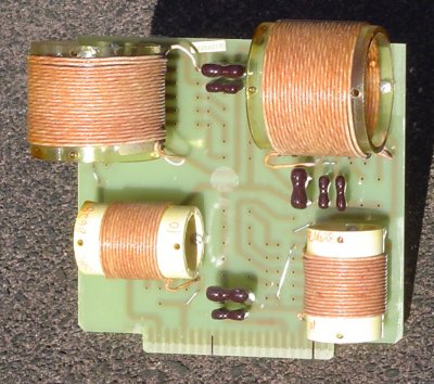
Note in the picture on the right, that the coils are all air wound.
Two each of two different inductors are used - the smaller ones (L1 and L4) are 35mm diameter, 30mm long, and measure 8.5µH with a Q of 82 at 550kHz.
The larger inductors, the two inner ones (L2 and L3) are 58mm diameter, 40mm long, and measure 31.5µH, with a Q of 110 at 550kHz. All inductors are Litz-wound, and the
inductors are mounted so that they are at right-angles to each other to minimize mutual coupling.
The capacitors are high voltage (1000V) mica types, made by CDE. The LP Filters plug in, and so can be easily changed to suit operation at other frequencies. Values (all resistors and capacitors) should be scaled to give the required cutoff frequency.
Combiner and SWR Sensing
The LP Filter mother board also carries two further transformers. Each is constructed of two stacked toroidal cores (see picture below), and are wound with Litz wire
with a 1.4:1 ratio (15 turns to 11 turns), so matching 50Ω input to 25Ω output. The primary of each transformer is driven by one of the transmitter modules through its LP filter. The secondaries are arranged in series so that the voltage contribution of each amplifier adds to the output, and the current is forced to be the same in each amplifier. The transformer secondaries are left floating, and the output
is not grounded until the SWR sensing module is reached.

See the SWR Sensor Schematic. One side of the combiner output is grounded on this small board,
which is mounted adjacent to the LP Filter mother board at the combiner end. The other side of the combiner output passes through the sensors. The transmitter signal enters
at the point labelled RF IN (top left). C1, C2 and R1 form a voltage sampler, providing a reference voltage and phase for the Forward and Reflected detectors. The two current transformers T1 and T2 are air-wound, about 15mm diameter, with a 1-turn primary. The secondaries are arranged in opposite phase where they sample the antenna voltage at the junction of C2 and R1. C2 is a mica compression trimmer, and can be adjusted to give minimum Reflected power into a 50Ω load. L1 and C3 form a low pass filter with a cutoff of about 180kHz, with the response broadened by R2 so that the overall response of the Forward power detector CR1 is approximately flat with frequency. The same applies to L2, R3 and CR2 for the Reflected power detector. R4, R5 and R6 form an antenna voltage sampler. CR3 provides a recified sample for modulation measurement. The outputs REFL and FWD are used by the monitor circuit and supplied to the SWR meter on the front panel of the transmitter drawer. MOD remains unused in this version (which has no AM modulation).
See the SWR Meter Schematic. The FWD and REFL signals enter at the left, pins 10 and 9, are attenuated (R2/R3, R5/R6) and operate unity gain buffer amplifiers U1C and U1D (LM324). The op-amp supply is +12V from the combined module supply, entering at pins 12 and 13 (+V, bottom left). The op-amps drive the meter via gain adjustment resistors R4, R7 and selector switch S2. The circuit board is mounted on the back of the rotary switch.
Power Supply
Each 500W transmitter module has its own power supply, which is physically mounted on top of its own large HV supply electrolytic capacitors.
See the Power Supply Schematic. The power supply is designed to operate with no break from AC or DC
supplies. For DC operation, the HV supply (+144V) arrives at screw connector pin 8 (144VDC IN, lower left). F2 is the DC supply fuse, and bridge CR6 acts to isolate the DC
supply from the AC supply when it is active. The HV AC supply is about 115V RMS, and arrives at screw terminals 1 and 2 (HVAC IN, lower left). After the line fuse F1, the AC is full-wave rectified by bridges CR4 and CR9 operating in parallel. These charge up the main reservoir capacitors C3 and C4 to about 165V (144V in DC operation). When AC power
is applied, the voltage on C3 and C4 exceeds the battery supply voltage and CR6 is reverse biassed, switching off the DC supply.
Relay K1 is a safety feature. When the AC and DC supplies fail, K1 drops out, placing R1 across the HV supply, discharging the capacitors in a matter of seconds. When DC power is provided, K1 is energized via R2, while CR7, a 5W Zener diode, clamps the relay supply at about 47V. When DC power fails the relay drops out quickly as C5 discharges. because CR6 is reverse biassed, no supply is available to the relay from C3 and C4. When AC power is provided, CR5 conducts, providing half-wave pulses to R2 which are clamped by CR7 and smoothed by C5. With half-wave supply the higher voltage from the AC supply causes less heating in R2 and CR7. High voltage output to the switching modulator is from screw terminal 5 (HVOUT, top right), with the HV ground at screw terminal 6. because the supply voltage drops from about 165V to 144V in battery operation, the power output of the transmitter drops about 15%. (Note that the Modulator/Regulator does not regulate the DC output - it provides a proportion of the DC input defined by the power setting, and so may not always regulate at the lower supply voltage).
Each transmitter module also requires a nominal 24V DC supply, which operates a 12V regulator supplying power to the module and a common 12V supply which powers shared circuitry, and common +24V unregulated supplying the cooling fan and some relays. DC supply from a battery enters at screw terminal 9 (+24V IN, top left), and passes through diode CR2 which disconnects the battery when AC power is supplied. The nominal 18V RMS AC supply enters at screw terminals 6 and 7 (LVAC IN, top left), and is full-wave rectified by bridge CR1. Approximately 25V is developed on smoothing capacitor C2, reverse biassing the DC supply diode CR2. The common 24V DC output at screw terminal 3 (24V OUT, top right) is ORed with the supply from the other module by diodes CR3 and the corresponding diode in the other module, and protected by fuse F3.
The +12V regulated supply is a switch-mode type for best efficiency. U3 is a single-chip switch-mode buck regulator controller, which uses CR8 and L1. When the power device in the chip is switched on, current is supplied to the load through L1. When the device is off, current is supplied from energy stored in L1, via CR8. U1 pin 4 senses the output voltage and adjusts the duty cycle of the internal switch accordingly. The +12V regulated output at screw terminal 1 (top right, +12V OUT) is smoothed by filter capacitor C2 and protected by fuse F4.
Monitor Circuits
This description is limited to those circuits provided in the transmitter drawer - not the automatic transfer and control provided by the RSIM Unit. Like the SWR Sensing board, the Monitor Control board is common to the two transmitters in the drawer. Only the circuitry described is operational in this transmitter - other parts of the Monitor Control board have to do with modulation. See the Monitor Control Schematic.
Adverse Reflected power will cause an immediate shutdown. Refected power is sensed at pin 16 (RFLS, top left) and compared with an adjustable threshold set by R2. When the threshold is exceeded, comparator U5 output goes high, setting RS latch U3B. The latch output goes high, and via NOR gate U4A and its inverter, reverse biasses CR11 and
sets the shutdown output at pin 19 high (SDO, bottom right).
Insufficient Forward power causes shutdown after a delay. Forward power is sensed at pin 22 (FWD, top left) and a sample adjusted by R6 is compared with a fixed threshold. Whenever the threshold not is exceeded, the comparator (formed by part of U1) output goes low, removing forward bias provided by R10 from the base of Q1 via CR7. With Q1 turned off, C6 is able to charge through R12 and R13, with the result that after about 25 seconds, unijunction transistor Q2 fires and sets RS latch U3C. As before, when the latch output goes high, the shutdown output SDO is set via NOR gate U4A.
The reset applied to pin 18 (RST, bottom left) causes inverter U5B to raise the reset inputs of latches U3B and U3C. If no fault condition exists, this then resets the latches and clears the shutdown output SDO. The Monitor switch on the front panel has three positions. In normal operation it is in the ENBL position (no connection) and SDO directly drives the Modulator shutdown, removing HV power when SDO is asserted. When the switch is set in the DSBL position, SDO is pulled low by the switch, preventing shutdown. At this time the front panel MON LED is lit, indicating over-ride. In the RST position of the switch, the RST input is momentarily pulled low, and the SDO shutdown mechanism operates normally.
The Module Disconnect Circuit monitors the PA, power supply, and Modulator HV fuse. One of
these small boards is provided for each 500W transmitter module. Screw terminal 4 (DRD, top left) samples the voltage at the output of the HV fuse in the modulator. This is compared with the HV supply at screw terminal 3 (HVIN, top left). Resistors R2 and R4 in the dividers are arranged so that the fuse sample is higher, and the output
of comparator U1A (terminal D) is normally high. D goes low when the fuse fails to indicate modulator failure.
Screw terminal 2 (DRS, bottom left) samples the voltage at the output of the HV fuse in the modulator. This is compared with the modulator output at screw terminal 1 (VMOD, bottom left). Resistors R2 and R4 in the dividers are arranged so that the fuse sample is higher, and the output
of comparator U1D (terminal S) is normally high. S goes low when the fuse fails, indicating PA failure.
The state of the HV supply is also checked to ensure that the power supply fuse is intact.
If it is, the HV sample will exceed the reference on pin 6 of U1B, set by resistors R5 and R6 at about 4V. Output H from U1B is normally high, and will go low when the
power supply fuse fails or the HV supply is below about 105V.
These three signals are used by the RSIM unit in determining change-over and status reporting, and are also used to indicate status on the front panel. A further LED
monitors the +12V supply from each transmitter module. If all is well, the HV and LV status LEDs for each transmitter will be on, and the PA Failure and Modulator Failure LEDs
will be off.
Rear Panel Signals
The following information is useful if a transmitter drawer is operated without the rest of the transmitter, or if the transmitter drawer alone has been replicated in some way. There are two coaxial connectors, and four 8-way terminal strips. To fire up the transmitter drawer alone, you only need connect up J1, J2 and TB1.
J1 MSK IN 0dBm carrier frequency drive, sinusoidal or square wave, AC coupled, 50Ω
J2 RF OUTPUT 1kW Transmitter output, 50Ω
TB1 POWER
- HVAC (115V)
- HVAC (115V)
- LVAC (18V)
- LVAC (18V)
- HVDC (+144V)
- GND
- GND
- LVDC (+24V)
TB2 STATUS
- SDOV (Not Shutdown)
- FWD (Forward Power)
- REFL (Reflected Power)
- SGV (not used)
- SSP (not used)
- NC
- NC
- GND
TB3 MONITOR
- MOD1 (Modulator fuse OK, module 1)
- PA1 (PA HV fuse, module 1)
- LV1 (+12V, module 1)
- HV1 (Supply fuse, module 1)
- MOD2 (Modulator fuse OK, module 2)
- PA2 (PA HV fuse, module 2)
- LV2 (+12V, module 2)
- HV2 (Supply fuse, module 2)
TB4 CONTROL
- SENSE (SDO2, shutdown)
- GND
- ACTRL +V (AC transformer enable switch)
- DCTRL +V (DC supply enable switch)
- AC CTRL (supply for AC transformer relay enable switch)
- DC CTRL (supply for HV battery supply relay enable switch)
- GND
- +12V (Common +12V supply)
Copyright � M. Greenman 1997-2005.
All rights reserved. Contact the author before using any of this material.
BACK
HOME