QUALITY ADJUSTABLE DC REGULATED LINEAR POWER SUPPLY 0-30V AND 0-3A
I Z33T home page I Z33T web pages in english I
Some time ago, I have been ordered "0-30V 2mA-3A Adjustable DC Regulated Power Supply DIY Kit" from China (via "ebay"). I decided to see what I will get and whether it will be good. I found that this cheap kit complete enables to build a very good quality laboratory power supply with features as it was advertised. Here's the schematics:
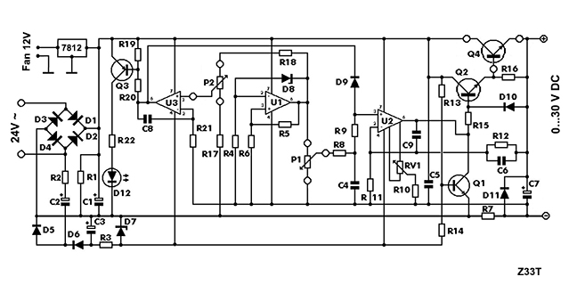
click on above schematics to see it in higher resolution
This DIY kit has an integrated voltage stabilizer (24V) with LM7824 for powering the cooling fan for additional cooling the output transistor Q4 (2SD1047) heat sink. Istead of the original LM7824, I have put LM7812, because it is easily to find 12V PC cooling fan than 24V one. In addition, this 12 Volt will be used for powering the Digital V/A meter with LED display which I puchased from ebay also. (it is very cheap and cost me 2.5 US dollars). One thing that I need to mention here is that the LM7812 have to be mounted on heat sink because it dissipates a lot of heat (depends of how big the cooling fan will be connected).
For this power supply unit to work properly it must be connected to 24V AC transformer (3 A). Do not try to connect 24V DC instead of AC becouse it does not work with DC voltage at the input.
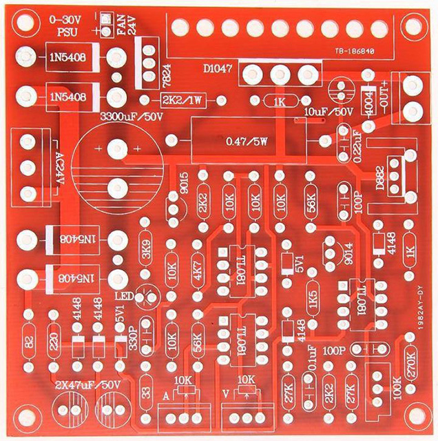
Be careful because some retailers on ebay sales this DIY kit with wrong prints for elements orientation on the PCB. I was ordered two DIY kits from two different sellers. On one PCB it was mistakenly wrong printed orientation of several diodes, and since the device did not work after I completed it, I had to investigated and find the problem. Corectly printed elements orientation on PCB looks like this:
With potentiometer P1, the output voltage can be set in range of 0V to 30V. In order to adjust the output voltage down to 0V, it is necessary to provide a negative voltage relative to the ground. The point between R3 and D7 is getting -5,1V negative voltage relative to the ground. This negative voltage is obtained by the elements R2, C2, D5, D6, C3, R3 and zener diode D7.
In order to avoid uncontrolled situations when this unit is powered on and off, the transistor Q1 is used which, together with the elements around it form a protective circuit. In a short period of time-off (while the negative voltage of -5,1V falls to zero) transistor Q1 switches off the voltage output, and no voltage is present at output terminals. This interesting solution cuts off the voltage at the device output terminals in case of AC input voltage of 24V falls down due to any reasons, automativcally protecting devices connected to this PSU. During normal operation, the transistor Q1 is nonconductive because the resistor R14 through the base of Q1 is held at negative voltage. But when negative voltage starts to falling down, the transistor Q1 becomes conductive (due to the positive voltage on its base through resistor R13), and thus connects the output of U2 to the ground and locks the transistor Q2, so it shut down the output voltage through Q4. Integrated circuit U2 has its own internal short-circuit protection on its output, so that this operation passes without any consequences. This solution is very important and inventive as the output voltage terminals of the PSU is switched off without waiting for large capacitors to discharge, which is a big advantage over the much more expensive factory laboratory power supply units.
Adjusting the potentiometer P2 you can set the maximum output current at the device terminals. In that way the device is protected against short-circuit on its output terminals. The output current can be set within the 2mA to 3A, which means that this unit can operate in constant current mode (regardless of how high is the voltage) which can be adjusted from 2mA to 3A! This feature can be very useful in the electronics laboratory. The limitation of the current is possible by the voltage drop on the resistor R7 which is connected in series with the connected load in output terminals. Integrated circuit U3 is in charge for this function. On his inverted input U3 compares the voltage at both ends of R7 with the voltage which is set by the P2 on noninverted input of the U3. If the voltage at the ends of R7, due to higher output current becomes greater than the voltage which is set to P2, then U3 comes into action, limiting the current and the entire device goes into a constant current regime, maintaining the output current constant and so accurate that it is possible to preset the current limit to as low as 2 mA. In that constant current regime, transistor Q3 becomes conductive, and LED D12 lights and signals it.The capacitor C8 is there to increase the stability of the circuit. Transistor Q3 is used to drive the LED whenever the current limiter is activated in order to provide a visual indication of the limiters operation.
The trimmer RV1 and the resistor R10 are used for the adjustment of the output voltages limits so that it can be reduced down to 0 V, despite any value tolerances of the other components in the circuit.
Voltage ripple from a 50Hz at output terminals is very small and not noticeable at low output current. In order to reduce voltage ripple at higher output current, another electrolytic capacitor with a larger capacity can be add in parallel to the capacitor C1 (eg 4700μF / 50 V), but it is not very necessary.
The output transistor Q4 disipates significant heat, especially at lower output voltages and higher output current and must be mounted on larger aluminum heat sink. The diference between DC input voltage (after bridge rectifier and capacitor C1) of about 33 volts and output voltage at the device output terminals, multiplied by the size of the output current is converted into heat in transistor Q4. That is why the Q4 disipates more heat at lower output voltages and higher output currents. Here is some calculations about disipation power on transistor Q4:
Example 1st
Let the output voltage is set to 30 Volts DC and connected load consumes 3 A (current limiter is set so that it can deliver current greater than or equal to 3 A). Transistor Q4 should disipates the following power:
(Uin - Uout) x Iout = (33-30) x 3 = 3 x 3 = 9W
Input voltage Uin is DC input voltage after bridge rectifier which is approximately equal to the AC voltage from the transformer multiplied by 1.41, so that 24V x 1.41 = 33V. It means thet the AC voltage of the transformer, from 24 volts becames 33 Volts DC after the bridge rectifier, at both ends of capacitor C1.
So in this example, the transistor Q4 will be disipates (converting into heat) about 9W.
Example 2nd
Let the output voltage is set to 1 Volts DC and connected load consumes 3 A (current limiter is set so that it can deliver current greater than or equal to 3 A). Transistor Q4 should disipates the following power:
(Uin - Uout) x Iout = (33-1) x 3 = 32 x 3 = 96W
Input voltage Uin is DC input voltage after bridge rectifier which is approximately equal to the AC voltage from the transformer multiplied by 1.41, so that 24V x 1.41 = 33V. It means thet the AC voltage of the transformer, from 24 volts becames 33 Volts DC after the bridge rectifier, at both ends of capacitor C1.
So in this example, the transistor Q4 will disipates (converting into heat) about 96W! (WARNING! it is too much heat, so big heat sink must be used or the transistor Q4 will be destroyed in very short time!)
Example 3rd
Let the output voltage is set to 13.8 Volts DC and connected load consumes 2 A (current limiter is set so that it can deliver current greater than or equal to 2 A). Transistor Q4 should disipates the following power:
(Uin - Uout) x Iout = (33-13.8) x 2 = 19.2 x 2 = 38.4W
Input voltage Uin is DC input voltage after bridge rectifier which is approximately equal to the AC voltage from the transformer multiplied by 1.41, so that 24V x 1.41 = 33V. It means thet the AC voltage of the transformer, from 24 volts becames 33 Volts DC after the bridge rectifier, at both ends of capacitor C1.
So in this example, the transistor Q4 will disipates (converting into heat) about 38.4W
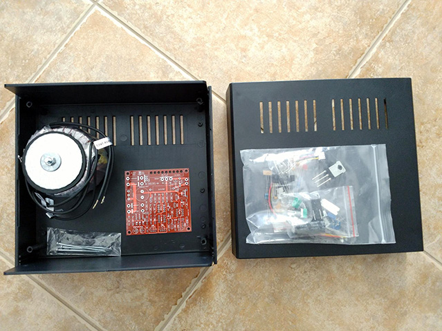
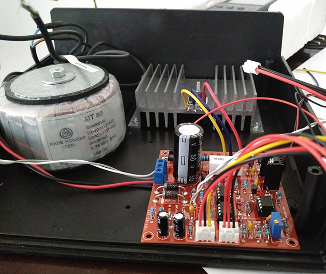
The following picture shows the Kit complete, the box in which elements will be placed and transformer 24V / 80VA:
The front panel of the box and elements planning:
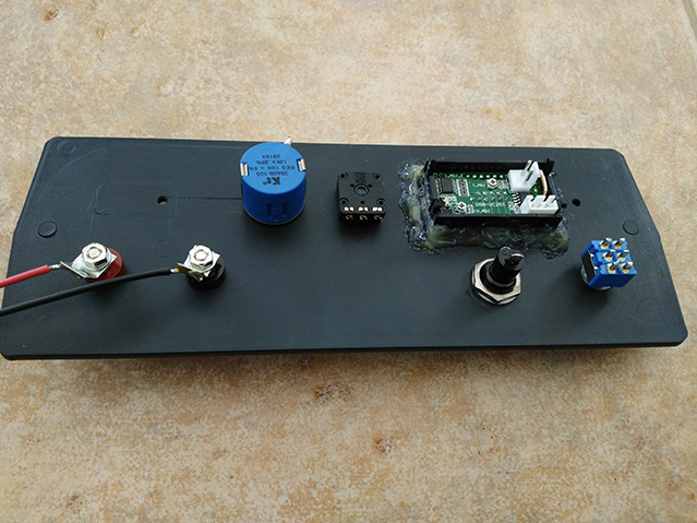
The original potentiometers which comes with the kit complete were good quality, but there where no screws for mounting at the front panel. Therefore I have used other potentiometers. For voltage regulation I have mount a multi turn potentiometer, so that can accurately adjust the desired output DC voltage. For adjusting the current limiter I have used ordinary linear potentiometer.
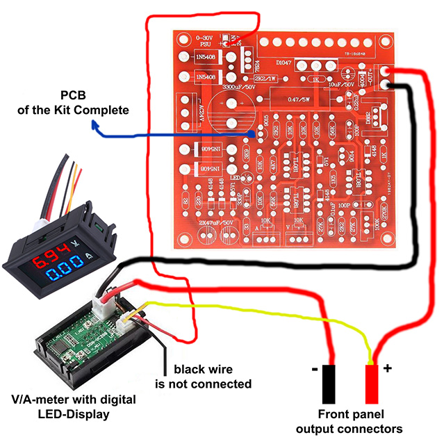
The wollowing picture shows how to connect Digital V/A-meter with LED Display:
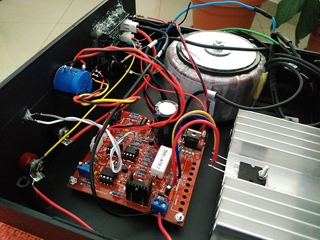
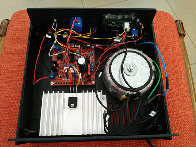
The wollowing pictures shows the finished device:
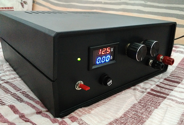
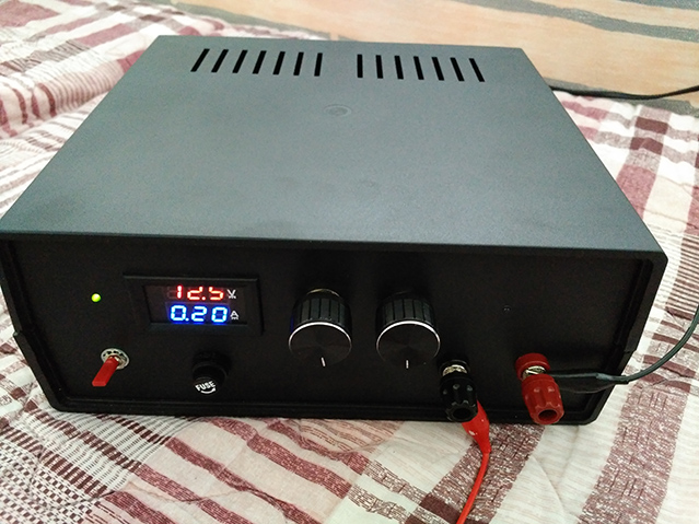
This Adjustable DC Regulated Power Supply with output voltage adjustment and current limiter proved to be an excellent device, which is far cheaper than similar that can be purchased on the market. It can be used to power many electric appliances in electronics laboratory. Moreover, the precise adjustment (current limiter) of output current provides an opportunity for this device to be used as a sofisticated charger for all kinds of batteries, which are best charged with constant current.
If you want this device to deliver higher output current (up to 5 or 6 A), the following changes shoul be done:
1. An appropriate transformer should be used which can provide 24V AC and 6A of AC current.
2. You need to add another similar output transistor Q5 in parallel with Q4, so that the bases of both transistors should be joined together, the collectors of the two transistors should be joined together, and from emitters of each transistor to the output positive teminal should be add one resistor 0.22 ohm / 3W, in order to balance the power load of the two parallel connected output transistors Q4 and Q5. These transistors have to be mounted on larger aluminum heat sink.
3. Diodes (1N5408) from bridge rectifier should be replaced by higher current ones, or instead of using 4 diodes, an adequate higher current bridge rectifier cab be used.
4. The resistor R7 (0,47 ohm - 5W) have to be replaced with 0.33 ohms - 12W resistor.
5. The resistor R18 (56k) that determines the maximum output current that then can be accurately limited to a lower value with potentiometer P2, should be replaced with 33k resistor.
6. For higher output current, it is necessary to put another electrolytic capacitor with a larger capacity in parallel to capacitor C1 (eg 4700μF / 50 V). It is best if you apply the rule that for every one ampere output current, it is necessary to predict at least 1000μF capacity for C1 capacitor.
- - - - - - - - - - - - - - - - - - - - - - - - - - - - - - - - - - - - -
The entire project cost me not more than 35 US dollars which is incomparable to similar PSU which are verey expensive.
- For DIY kit complete, try to find on ebay as "0-30V 2mA-3A Adjustable DC Regulated Power Supply DIY Kit" (it cost me 6.4 US dollars)
- For Digital V/A-meter with LED display, try to find on ebay as "DC 100V 10A Voltmeter Ammeter Blue + Red LED Dual Digital Volt Amp Meter" (it cost me 2.5 US dollars)
Beside this, you need the transformer 24V/3A, an adequate plastic or metal box, aluminum heat sink, switch for on and off and output terminals.
Good Luck!
I Z33T home page I Z33T web pages in english I