At the left of the drawing is a 14MHz TCXO. These can be obtained on a range of suitable frequencies, sometimes surplus
(for example 14.85MHz units are used in many cellular phones). Any frequency from 14 to 15MHz will be suitable for 80m
use (depends on the Amateur band allocation in your country). If you build this transmitter, MAKE SURE that the oscillator
you use is a TCXO, not just a packaged oscillator. Many old computer cards include such oscillators, and some will
be on 14.31818MHz - very tempting, but don't be fooled - they are not stable enough.
The output of the TCXO is typically AC coupled, and a clipped sinewave about 1V p-p. This is insufficient to drive CMOS directly,
but if biassed to half-supply by two 100k resistors, will reliably clock the first 74HC74 divider, U1A. This D flip-flop is arranged
to divide by two through the expedient of connecting the /Q inverting output to the D input. If you are lucky enough to
locate a TCXO with CMOS output, just omit the two resistors.
The second flip-flop, U1B, is also arranged to divide by two. In this case the /CLR (reset) input (pin 13) is held high by a resistor, and
when power is applied, the capacitor on this pin holds the divider in reset (Q output low) until after the TCXO has reliably
started. The 10nF capacitor charges to 5V through the 100k resistor to remove reset after about 1ms. Without this addition,
the divider might randomly start with the output high, and since the TCXO may take up to several hundred µs to
start, the PA stage could be turned hard on and draw excessive current. If necessary, the transmitter may be turned on and off by
connecting a switch from this point (U1B pin 13) to ground. Keying the transmitter for ID purposes at this point may however
lead to strong key clicks, and the logic is inverted from that of a normal key (which keys to ground to transmit).
Power for the CMOS device and the TCXO is derived from a simple shunt regulator. Zener diode D1 holds the voltage at about 4.7V,
using current from the 12V supply via the 470 Ω resistor. If you wish, you could use two red LEDs and a 1N4002 in series
in place of the Zener diode to achieve about 4.7V, and have a front panel LED power indicator at no extra current drain. The
shunt regulator, TCXO and divider draw about 15 to 20mA in total. Most of the current goes into driving the PA gate circuit.
The PA stage draws about 80mA for an input power of about 900mW.
The PA stage is shown at the right (power FET Q1), and is gate driven with a 50% duty cycle waveform.
Capacitive coupling ensures that the transistor turns off if
drive is inadvertently lost, as always happens briefly at switch-on. The resistor to ground ensures that the transistor stays off
without drive.
The diode D2 is a clamp which ensures that the drive is all positive, 0 - 4V, rather than -2V to +2V. This type of FET has a switch-on voltage of about 2.5V, and can be adequately driven by a single CMOS gate. Don't use bigger FETs as the gate capacitance will be too
large for the CMOS driver to handle. If smaller FETs (such as 2N7000) are contemplated, use several parallel devices to achieve
sufficiently low on resistance - otherwise the FET will get rather hot.
The chosen FET is a small surface-mount N-channel power FET, 200V at 9A peak, with a low on resistance (about 0.3Ω). In this
application the FET is virtually indestructable, and needs only a small heatsink (small clip-on type or 400mm2 of
PCB copper). The FET conducts with close to 50% duty cycle, and has an input capacitance of about 700pF. Larger FETs, such as IRF510
or IRF740 may not be adequately driven by such a simple circuit.
The output circuit is arranged as a simple Class E type. The inductor in the drain supply and the combination of the output
circuit and FET drain capacitance resonates at the operating frequency. When the FET conducts, the FET current
describes a half-sine, while the drain voltage is essentially zero, and when it does not
conduct, the drain voltage describes an approximate half-sine peaking at twice the supply voltage. Thus the device is very
efficient - power is lost only to switching transients and ohmic effects.
The FET output capacitance is nominally about 250pF at 12V, but swings from 150pF at 24V to nearly 900pF close to 0V,
so the output tank circuit matching varies as the voltage varies. Ideally shunting the FET with a large capacitance to resonate
with the series inductor minimizes this effect, which is prone to generation of harmonics. This simple design is something
of a compromise, aimed at simplicity rather than power output and optimum matching.
Following the tank circuit, and to some extent part of it, is a low pass filter, and with just a single stage filter
the output is reasonably sinusoidal
into a 50Ω load. If the load deviates from 50Ω, the waveform deteriorates, and it would be best to use an antenna
tuner or extra filter stages. The capacitor on the FET side of the output low pass filter will need to be adjusted to give the best
wave shape, and depends on the FET used (output capacitance) and the supply voltage. You could try putting it on the FET side
of the 2n2 blocking capacitor. Use a broadcast variable capacitor to start with. In the prototype, this capacitor was not needed
at all because of high FET output capacitance.
The two inductors in the prototype were bobbin wound. The filter inductor could be a 12mm toroidal core, but the bobbin
arrangement is best for the drain inductor, as the leakage inductance prevents saturation caused by the DC component.
Most users will be required by regulations to provide regular identification of beacon transmitters, even at low power level.
Achieving good ID and at the same time clean Spectrograms is something of a compromise. Two techniques are known to be successful:
- Use ASK keying at about 10dB power-drop. In other words, drop the power 10dB and key it back up again. There will
be some keying sidebands, but provided the keying speed is 10WPM or greater, the sidebands will be outside the Spectrogram.
By limiting the keying depth, the keying sideband strength is reduced.
- Use high-level AM modulation at low modulation depth. If say the transmitter is MCW modulated using a keyed 500Hz tone,
the carrier power will change little, and all the keying energy should be centred 500Hz either side of the transmission.
This technique may not be legal on 80m in all countries.
There are many automatic ID keyer designs around. The designer of course recommends the
ZL1BPU Mini-Keyer. It generates both DC keying and
980Hz audio tone keying in several Morse and Hellschreiber modes. The separate PTT output can be used to drop the power prior
to keying it up again, then restoring it after keying.
The transmitter can be ASK keyed for ID purposes by keying the supply to the FET at the point marked 'X' (preferably don't also
key the 5V supply via the 470Ω resistor). Use another power FET as keying device. Connect an 82Ω 1W resistor across the
FET or key to reduce keying depth (adds 'backwave') and a 1uF capacitor across the 100nF capacitor shown to minimize keying clicks
and give a clean spectrum through the ID. Adjust the 82Ω resistor value for appropriate keying depth. If the FET has a heatsink,
you could omit the 82Ω resistor and use a 10kΩ pull-up resistor on the gate to the drain to turn it on, and a 10kΩ
variable resistor to the keying source, adjusted to set the lower power level.
Another sneaky way to achieve a similar result is to use an LM317 regulator, set for 12V, and key the reference pin
to ground via a resistor to drop the power. Start with a 15V supply before the regulator. The regulator of course
only powers the PA stage, at point X.
The transmitter can also be easily high-level AM modulated at the point marked 'X', using a series modulation transformer, with an added
100uF electrolytic bypass capacitor on the supply above the point 'X'. With 12V DC applied to the transmitter, the peak transmitter output
power could be more than 1W on modulation peaks. For full modulation about 1W of audio will be required, and the modulating
impedance is about 100Ω. For propagation monitoring purposes however, it's best to keep the modulation down at about 30%. Adjust the
audio level to give the highest sideband power with no trace of keying within 10Hz of the carrier.
Before powering up the unit, disconnect point 'X'. Apply power from a variable supply, and check that you don't get more than 5V
at the Zener diode D1. As you increase the supply voltage, you may find that at first the voltage climbs, then drops away as the oscillator starts (U1 draws more current), and then returns to nearly 5V as the supply climbs to 12V. Check the 80m signal on a receiver, and ensure
that the carrier is stable and does not drop out after a while.
Connect up point 'X', and with a dummy load attached, increase the supply from 5V to 12V, while watching the current. It should
remain below 100mA. Preferably watch the output waveform on a spectrum analyser or oscilloscope, and adjust the capacitor in
the output for lowest harmonic content (best sine wave). This should also coincide with highest output power on 80m and lowest transmitter
current (rather like 'dipping the final' of an old steam-powered transmitter). Adjustment is easiest using a two-gang BC variable capacitor (2 x 250pF) with the sections in parallel. Once you have the right value, replace the capacitor with a fixed value. Use 100V
polystyrene caps for lowest loss and best stability. Don't be surprised if the best results are with no added capacitance!
Once everything is working to your satisfaction, assemble the unit in a diecast metal box, preferably with a heat transfer method
from FET to case (a TO-220 device would make this easier, but remember the tab is live to the drain and will need insulating).
Heat transfer direct to the case means less heat inside the box to cause TCXO variations.
In operation, mount the unit in a small polystyrene box, or a recess cut from a polystyrene slab, to slow down thernal variations.
Because the transmiter power level is low, unless you have a QRP SWR bridge or antenna bridge, it might be best to tune up the
antenna at the operating frequency with a normal higher powered transmitter. Then change to the little transmitter, and away you go!
Check that the current drawn is similar to that on the dummy load. You may be able to tweak the antenna tuner slightly for
least transmitter current or maximum antenna current.
A first deployment should be at a friend's place nearby. Then you can check the ground-wave signal for long term stability,
while enjoying watching the NVIS effects caused by the F-layer. In the picture below, you can see how stable the transmitter
and receiver are, by the ruler-straight ground wave signal. The other fuzzy stuff is NVIS F-layer propagation.
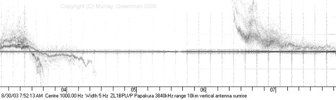
NVIS 80m propagation at 10km range (overnight)
The transmitter will run for almost a week from a 7AH SLA battery. The transmitter output power can be increased considerably
by increasing the supply voltage to 15 - 20V, but the series regulator resistor should also be increased in value. At 20V, the
power output will be close to 2W. I don't suggest combining AM modulation with 20V supply as this will stretch the safe operating
parameters of the FET too much. The 500mW signal can be received using a Spectrogram at 1000km range, even during the day.
Copyright © Murray Greenman 1997-2005.
All rights reserved. Contact the author before using any of this material.
