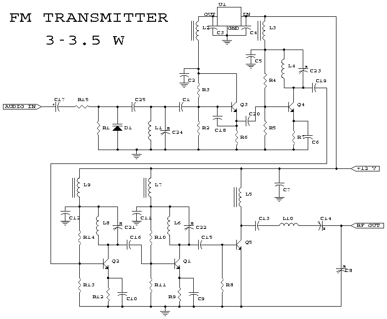
FM transmitter
This is a circuit that I've build a few years ago for a friend, who used it in combination with the BLY88 amplifier to obtain 20 W output power. From the notes that I made at the original schematic, it worked fine with a SWR of 1 : 1.05 (quite normal at my place with my antenna).

|
|
|
|
|
| R1,R4,R14,R15 | 4 | 10K 1/4W Resistor | |
| R2,R3 | 2 | 22K 1/4W Resistor | |
| R5,R13 | 2 | 3.9K 1/4W Resistor | |
| R6,R11 | 2 | 680 Ohm 1/4W Resistor | |
| R7 | 1 | 150 Ohm 1/4W Resistor | |
| R8,R12 | 2 | 100 Ohm 1/4W Resistor | |
| R9 | 1 | 68 Ohm 1/4W Resistor | |
| R10 | 1 | 6.8K 1/4W Resistor | |
| C1 | 1 | 4.7pF Ceramic Disc Capacitor | |
| C2,C3,C4,C5,C7,C11,C12 | 7 | 100nF Ceramic Disc Capacitor | |
| C6,C9,C10 | 3 | 10nF Ceramic Disc Capacitor | |
| C8,C14 | 2 | 60pF Trimmer Capacitor | |
| C13 | 1 | 82pF Ceramic Disc Capacitor | |
| C15 | 1 | 27pF Ceramic Disc Capacitor | |
| C16 | 1 | 22pF Ceramic Disc Capacitor | |
| C17 | 1 | 10uF 25V Electrolytic Capacitor | |
| C18 | 1 | 33pF Ceramic Disc Capacitor | |
| C19 | 1 | 18pF Ceramic Disc Capacitor | |
| C20 | 1 | 12pF Ceramic Disc Capacitor | |
| C21,C22,C23,C24 | 4 | 40pF Trimmer Capacitor | |
| C25 | 1 | 5pF Ceramic Disc Capacitor | |
| L1 | 1 | 5 WDG, Dia 6 mm, 1 mm CuAg, Space 1 mm | |
| L2,L3,L5,L7,L9 | 5 | 6-hole Ferroxcube Wide band HF Choke (5 WDG) | |
| L4,L6,L8 | 3 | 1.5 WDG, Dia 6 mm, 1 mm CuAg, Space 1 mm | |
| L10 | 1 | 8 WDG, Dia 5 mm, 1 mm CuAg, Space 1 mm | |
| D1 | 1 | BB405 | BB102 or equal (most varicaps with C = 2-20 pF [approx.] will do) |
| Q1 | 1 | 2N3866 | |
| Q2,Q4 | 2 | 2N2219A | |
| Q3 | 1 | BF115 | |
| Q5 | 1 | 2N3553 | |
| U1 | 1 | 7810 Regulator | |
| MIC | 1 | Electret Microphone | |
| MISC | 1 | PC Board, Wire For Antenna, Heatsinks |
2. Q1 and Q5 should be cooled with a heat sink. The case-pin of Q4 should be grounded.
3. C24 is for the frequency adjustment. The other trimmers must be adjusted to maximum output power with minimum SWR and input current.
[ About me
| Acronyms | CW
| Data Sheets | Docs
| Download | E-mail
| HOME | Ham
projects | Hobby circuits
| Photo galery | PIC
| QTH
photos |
Sign
in my guestbook | View
my guestbook ]
© 2001 - YO5OFH, Csaba Gajdos