
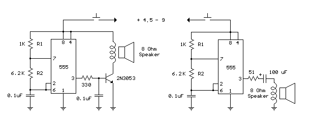
555 Tone Generator (8 ohm speaker)

This is a basic 555 squarewave oscillator used to produce a 1 Khz tone from an 8 ohm speaker. In the circuit on the left, the speaker is isolated from the oscillator by the NPN medium power transistor which also provides more current than can be obtained directly from the 555 (limit = 200 mA). A small capacitor is used at the transistor base to slow the switching times which reduces the inductive voltage produced by the speaker. Frequency is about 1.44/(R1 + R2)C where R1 (1K) is much smaller than R2 (6.2K) to produce a near squarewave. Lower frequencies can be obtained by increasing the 6.2K value, higher frequencies will probably require a smaller capacitor as R1 cannot be reduced much below 1K. Lower volume levels can be obtained by adding a small resistor in series with the speaker (10-100 ohms). In the circuit on the right, the speaker is directly driven from the 555 timer output. The series capacitor (100 uF) increases the output by supplying an AC current to the speaker and driving it in both directions rather than just a pulsating DC current which would be the case without the capacitor. The 51 ohm resistor limits the current to less than 200 mA to prevent overloading the timer output at 9 volts. At 4.5 volts, a smaller resistor can be used.
Original scheme edited by Bill
Bowden, http://www.bowdenshobbycircuits.info
Generating -5 Volts From a 9 Volt Battery
A 555 timer can be used to generate a squarewave to produce a negative voltage relative to the negative battery terminal.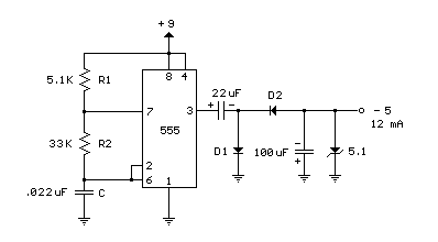 When the timer output at pin 3 goes positive, the series 22 uF capacitor charges through the diode (D1) to about 8 volts. When the output switches to ground, the 22 uF cap discharges through the second diode (D2) and charges the 100 uF capacitor to a negative voltage. The negative voltage can rise over several cycles to about -7 volts but is limited by the 5.1 volt zener diode which serves as a regulator. Circuit draws about 6 milliamps from the battery without the zener diode connected and about 18 milliamps connected. Output current available for the load is about 12 milliamps. An additional 5.1 volt zener and 330 ohm resistor could be used to regulate the +9 down to +5 at 12 mA if a symmetrical +/- 5 volt supply is needed. The battery drain would then be around 30 mA. When the timer output at pin 3 goes positive, the series 22 uF capacitor charges through the diode (D1) to about 8 volts. When the output switches to ground, the 22 uF cap discharges through the second diode (D2) and charges the 100 uF capacitor to a negative voltage. The negative voltage can rise over several cycles to about -7 volts but is limited by the 5.1 volt zener diode which serves as a regulator. Circuit draws about 6 milliamps from the battery without the zener diode connected and about 18 milliamps connected. Output current available for the load is about 12 milliamps. An additional 5.1 volt zener and 330 ohm resistor could be used to regulate the +9 down to +5 at 12 mA if a symmetrical +/- 5 volt supply is needed. The battery drain would then be around 30 mA.
Original scheme edited by Bill
Bowden, http://www.bowdenshobbycircuits.info
Transistor / Diode / IC (DIP) Outlines
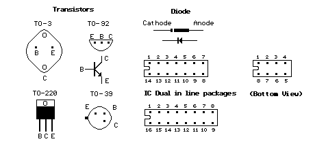
Original scheme edited by Bill
Bowden, http://www.bowdenshobbycircuits.info
The 555 Timer
First introduced by the Signetics Corporation as the SE555/NE555 about 1971.
Pin connections and functions: (See schematic below for basic circuits)
Pin 1 (Ground) - The ground (or common) pin is the most-negative supply potential of the device, which is normally connected to circuit common when operated from positive supply voltages.
Pin 2 (Trigger) - This pin is the input which causes the output to go high and begin the timing cycle. Triggering occurs when the trigger input moves from a voltage above 2/3 of the supply voltage to a voltage below 1/3 of the supply. For example using a 12 volt supply, the trigger input voltage must start from above 8 volts and move down to a voltage below 4 volts to begin the timing cycle. The action is level sensitive and the trigger voltage may move very slowly. To avoid retriggering, the trigger voltage must return to a voltage above 1/3 of the supply before the end of the timing cycle in the monostable mode. Trigger input current is about 0.5 microamps.
Pin 3 (Output) - The output pin of the 555 moves to a high level of 1.7 volts less than the supply voltage when the timing cycle begins. The output returns to a low level near 0 at the end of the cycle. Maximum current from the output at either low or high levels is approximately 200 mA.
Pin 4 (Reset): - A low logic level on this pin resets the timer and returns the ouput to a low state. It is normally connected to the + supply line if not used.
Pin 5 (Control) - This pin allows changing the triggering and threshold voltages by applying an external voltage. When the timer is operating in the astable or oscillating mode, this input could be used to alter or frequency modulate the output. If not in use, it is recommended installing a small capacitor from pin 5 to ground to avoid possible false or erratic triggering from noise effects.
Pin 6 (Threshold) - Pin 6 is used to reset the latch and cause the output to go low. Reset occurs when the voltage on this pin moves from a voltage below 2/3 of the supply to a voltage above 2/3 of the supply. The action is level sensitive and can move slowly similar to the trigger voltage.
Pin 7 (Discharge) - This pin is an open collector output which is in phase with the main output on pin 3 and has similar current sinking capability.
Pin 8 (V +) - This is the positive supply voltage terminal of the 555 timer IC. Supply-voltage operating range is +4.5 volts (minimum) to +16 volts (maximum).
The pin connections for the 556 which is a dual 555 timer (2 in one package) are shown in table below. For example, the two outputs for the two timers of the 556 are on pins 5 and 9 which correspond to the output pin 3 of the 555.
| |
555 |
556 - Timer 1 |
556 - Timer 2 |
| Ground |
1 |
7 |
7 |
| Trigger |
2 |
6 |
8 |
| Output |
3 |
5 |
9 |
| Reset |
4 |
4 |
10 |
| Control |
5 |
3 |
11 |
| Threshold |
6 |
2 |
12 |
| Discharge |
7 |
1 |
13 |
| + Vcc |
8 |
14 |
14 |
The schematics below show the two basic circuits for the 555 timer.
Positive Time Interval (T1) = 0.693 * (R1+R2) * C
Negative Time Interval (T2) = 0.693 * R2 * C
Frequency = 1.44 / ( (R1+R2+R2) * C)
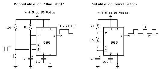
Original scheme edited by Bill
Bowden, http://www.bowdenshobbycircuits.info
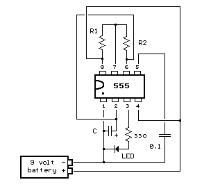 Below is a pictorial view of the 555 timer wired as a LED flasher and powered with a 9 volt battery. The LED will turn on during time T1 and off during time T2. Below is a pictorial view of the 555 timer wired as a LED flasher and powered with a 9 volt battery. The LED will turn on during time T1 and off during time T2.
The 555 circuit below is a flashing bicycle light powered with three C or D cells (4.5 volts). The two flashlight lamps will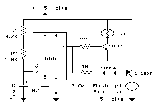 alternately flash at a approximate 1.5 second cycle rate. Using a 4.7K resistor for R1 and a 100K resistor for R2 and a 4.7uF capacitor, the time intervals for the two lamps are 341 milliseconds (T1, upper lamp) and 326 milliseconds (T2 lower lamp). The lamps are driven by transistors to provide additional current beyond the 200 mA limit of the 555 timer. A 2N2905 PNP and a 2N3053 NPN could be used for lamps requiring 500 mA or less. For additional current, a TIP29 NPN and TIP30 PNP could be used up to 1 amp. A PR3 is a 4.5 volt, 500 mA flashlight bulb. Two diodes are placed in series with the PNP transistor base so that the lower lamp turns off when the 555 output goes high during the T1 time interval. The high output level of the 555 timer is 1.7 volts less than the supply voltage. Adding the two diodes increases the forward voltage required for the PNP transistor to about 2.1 volts so that the 1.7 volt difference from supply to the output is not enough to turn on the transistor. You can also use an LED in place of the two diodes as shown in the lower schematic. alternately flash at a approximate 1.5 second cycle rate. Using a 4.7K resistor for R1 and a 100K resistor for R2 and a 4.7uF capacitor, the time intervals for the two lamps are 341 milliseconds (T1, upper lamp) and 326 milliseconds (T2 lower lamp). The lamps are driven by transistors to provide additional current beyond the 200 mA limit of the 555 timer. A 2N2905 PNP and a 2N3053 NPN could be used for lamps requiring 500 mA or less. For additional current, a TIP29 NPN and TIP30 PNP could be used up to 1 amp. A PR3 is a 4.5 volt, 500 mA flashlight bulb. Two diodes are placed in series with the PNP transistor base so that the lower lamp turns off when the 555 output goes high during the T1 time interval. The high output level of the 555 timer is 1.7 volts less than the supply voltage. Adding the two diodes increases the forward voltage required for the PNP transistor to about 2.1 volts so that the 1.7 volt difference from supply to the output is not enough to turn on the transistor. You can also use an LED in place of the two diodes as shown in the lower schematic.
Original scheme edited by Bill
Bowden, http://www.bowdenshobbycircuits.info
Set/Reset Flip Flop
 This is an example of a set/reset flip flop using discrete components. When power is applied, only one of the transistors will conduct causing the other to remain off. The conducting transistor can be turned off by grounding it's base through the push button which causes the collector voltage to rise and turn on the opposite transistor. This is an example of a set/reset flip flop using discrete components. When power is applied, only one of the transistors will conduct causing the other to remain off. The conducting transistor can be turned off by grounding it's base through the push button which causes the collector voltage to rise and turn on the opposite transistor.
Original scheme edited by Bill
Bowden, http://www.bowdenshobbycircuits.info
Bistable Flip Flop
Here are two examples of bistable flip flops which can be toggled between states with a single push button. When the button is pressed, the capacitor connected to the base of the conducting transistor will charge to a slightly higher voltage. When the button is released, the same capacitor will discharge back to the previous voltage causing the transistor to turn off. The rising voltage at the collector of the transistor that is turning off causes the opposite transistor to turn on and the circuit remains in a stable state until the next time the button is pressed and released. Note that in the LED circuit, the base current from the conducting transistor flows through the LED that should be off, causing it to illuminate dimly. The base current is around 1 mA and adding a 1K resistor in parallel with the LED will reduce the voltage to about 1 volt which should be low enough to ensure the LED turns completely off.
Original scheme edited by Bill
Bowden, http://www.bowdenshobbycircuits.info

High Current MOSFET Toggle Switch with Debounced Push Button.
This circuit was adapted from the "Toggle Switch Debounced Pushbutton" by John Lundgren. It is particularly useful in controlling a load from several locations where the load may be switched on from one location and switched off from another. Any number of momentary (N/O) switches or push buttons may be connected in parallel.
The circuit uses a N-channel power MOSFET to control the load and can supply fairly large currents depending on the MOSFET used. The IRFZ44 is a 50 amp device available at Radio Shack for $2.99 and the IRF10 is a 4 amp device available for a dollar less.
The combination (10K, 10uF and diode) on the left side of the schematic insures the circuit powers on with the MOSFET turned off and the NPN transistor conducting. These components can be omitted if the initial power-on condition is not a concern. In this initial state (MOSFET off), the voltage at the gate of the MOSFET will be near zero and the voltage on the 1uF capacitor connected to the switches will also be near zero.
When a switch is closed, the 1uF capacitor is connected to the junction of the 220 ohm and 470K resistors causing the voltage to fall to near zero turning off the NPN transistor. As the transistor turns off, the collector voltage rises and turns on the MOSFET when the voltage climbs above about 3 volts. The drain terminal (D) of the MOSFET now moves close to ground preventing the NPN transistor from turning back on. When the switch is opened, the 1uF cap will charge through the 4.7M and 10K resistors to the full supply voltage. When a switch is again closed, the 1uF capacitor will cause the NPN transistor to turn back on due to the positive voltage on the capacitor applied to the junction of the two resistors (470K, 220). The MOSFET will now turn off and the drain voltage will rise to the supply voltage which in turn keeps the NPN transistor conducting with a positive voltage on the base. The circuit has now returned to the initial turn-on state.
The small (0.1uF) capacitor connected from the transistor base to ground functions to filter out noise that could cause false triggering if the switches are located far away from the circuit using long wires. If false triggering becomes a problem, either the capacitor value (0.1) or the 220 ohm resistor value can be increased to provide better filtering. Increasing these values however will increase the switching times of the MOSFET (rise and fall times) generating more heat when the MOSFET changes state. This is probably not a problem with small loads of a couple amps or less, but may be a problem at higher load currents. The circuit was tested at 1.5 amps using the IRF510 and 6 amps using the IRFZ44.
Original scheme edited by Bill
Bowden, http://www.bowdenshobbycircuits.info
Monostable Flip Flop
The monostable flip flop, sometimes called a 'one shot' is used to produce a single pulse each time it is triggered. It can be used to debounce a mechanical switch so that only one rising and one falling edge occurs for each switch closure, or to produce a delay for timing applications. In the discrete circuit, the left transistor normally conducts while the right side is turned off. Pressing the switch grounds the base of the conducting transistor causing it to turn off which causes the collector voltage to rise. As the collector voltage rises, the capacitor begins to charge through the base of the opposite transistor, causing it to switch on and produce a low state at the output. The low output state holds the left transistor off until the capacitor current falls below what is needed to keep the output stage saturated. When the output side begins to turn off, the rising voltage causes the left transistor to return to it's conducting state which lowers the voltage at it's collector and causes the capacitor to discharge through the 10K resistor (emitter to base). The circuit then remains in a stable state until the next input. The one shot circuit on the right employs two logic inverters which are connected by the timing capacitor. When the switch is closed or the input goes negative, the capacitor will charge through the resistor generating an initial high level at the input to the second inverter which produces a low output state. The low output state is connected back to the input through a diode which maintains a low input after the switch has opened until the voltage falls below 1/2 Vcc at pin 3 at which time the output and input return to a high state. The capacitor then discharges through the resistor (R) and the circuit remains in a stable state until the next input arrives. The 10K resistor in series with the inverter input (pin 3) reduces the discharge current through the input protection diodes. This resistor may not be needed with smaller capacitor values.
Note: These circuits are not re-triggerable and the output duration will be shorter than normal if the circuit is triggered before the timing capacitors have discharged which requires about the same amount of time as the output. For re-triggerable circuits, the 555 timer, or the 74123 (TTL), or the 74HC123 (CMOS) circuits can be used.
Original scheme edited by Bill
Bowden, http://www.bowdenshobbycircuits.info
Transistor Schmitt Trigger Oscillator
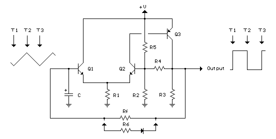 The Schmitt Trigger oscillator below employs 3 transistors, 6 resistors and a capacitor to generate a square waveform. Pulse waveforms can be generated with an additional diode and resistor (R6). Q1 and Q2 are connected with a common emitter resistor (R1) so that the conduction of one transistor causes the other to turn off. Q3 is controlled by Q2 and provides the squarewave output from the collector. The Schmitt Trigger oscillator below employs 3 transistors, 6 resistors and a capacitor to generate a square waveform. Pulse waveforms can be generated with an additional diode and resistor (R6). Q1 and Q2 are connected with a common emitter resistor (R1) so that the conduction of one transistor causes the other to turn off. Q3 is controlled by Q2 and provides the squarewave output from the collector.
In operation, the timing capacitor charges and discharges through the feedback resistor (Rf) toward the output voltage. When the capacitor voltage rises above the base voltage at Q2, Q1 begins to conduct, causing Q2 and Q3 to turn off, and the output voltage to fall to 0. This in turn produces a lower voltage at the base of Q2 and causes the capacitor to begin discharging toward 0. When the capacitor voltages falls below the base voltage at Q2, Q1 will turn off causing Q2 and Q3 to turn on and the output to rise to near the supply voltage and the capacitor to begin charging and repeating the cycle. The switching levels are established by R2,R4 and R5. When the output is high, the voltage at the base of Q2 is determined by R4 in parallel with R5 and the combination in series with R2. When the output is low, the base voltage is set by R4 in parallel with R2 and the combination in series with R5. This assumes R3 is a small value compared to R2. The switching levels will be about 1/3 and 2/3 of the supply voltage if the three resistors are equal (R2,R4,R5).
There are many different combinations of resistor values that can be used. R3 should low enough to pull the output signal down as far as needed when the circuit is connected to a load. So if the load draws 1mA and the low voltage needed is 0.5 volts, R3 would be 0.5/.001 = 500 ohms (510 standard). When the output is high, Q3 will supply current to the load and also current through R3. If 10 mA is needed for the load and the supply voltage is 12, the transistor current will be 24 mA for R3 plus 10 mA to the load = 34 mA total. Assuming a minimum transistor gain of 20, the collector current for Q2 and base current for Q3 will be 34/20 = 1.7 mA. If the switching levels are 1/3 and 2/3 of the supply (12 volts) then the high level emitter voltage for Q1 and Q2 will be about 7 volts, so the emitter resistor (R1) will be 7/0.0017 = 3.9K standard. A lower value (1 or 2K) would also work and provide a little more base drive to Q3 than needed. The remaining resistors R2, R4, R5 can be about 10 times the value of R1, or something around 39K.
The combination of the capacitor and the feedback resistor (Rf) determines the frequency. If the switching levels are 1/3 and 2/3 of the supply, the half cycle time interval will be about 0.693*Rf*C which is similar to the 555 timer formula. The unit I assembled uses a 56K and 0.1 uF cap for a positive time interval of about 3.5 mS. An additional 22K resistor and diode were used in parallel with the 56K to reduce the negative time interval to about 1 mS.
In the diagram, T1 represents the time at which the capacitor voltage has fallen to the lower trigger potential (4 volts at the base of Q2) and caused Q1 to switch off and Q2 and Q3 to switch on. T2 represents the next event when the capacitor voltage has risen to 8 volts causing Q2 an Q3 to turn off and Q1 to conduct. T3 represents the same condition as T1 where the cycle begins to repeat. Now, if you look close on a scope, you will notice the duty cycle is not exactly 50% This is due to the small base current of Q1 which is supplied by the capacitor. As the capacitor charges, the E/B of Q1 is reverse biased and the base does not draw any current from the capacitor so the charge time is slightly longer than the discharge. This problem can be compensated for with an additional diode and resistor as shown (R6) with the diode turned around the other way.
Original scheme edited by Bill
Bowden, http://www.bowdenshobbycircuits.info
Generating Long Time Delays
Generating long delays of several hours can be accomplished by using a low frequency oscillator and a binary counter as shown below. A single Schmitt Trigger inverter stage (1/6 of 74HC14) is used as a squarewave oscillator to produce a low frequency of about 0.5 Hertz. The 10K resistor in series with the input (pin 1) reduces the capacitor discharge current through the inverter input internal protection diodes if the circuit is suddenly disconnected from the supply. This resistor may not be needed but is a good idea to use.
The frequency is divided by two at each successive stage of the 12 stage binary counter (CD4040) which yields about 1 hour of time before the final stage (Q12) switches to a high state. Longer or shorter times can be obtained by adjusting the oscillator frequency or using different RC values. Each successive stage changes state when the preceding stage switches to a low state (0 volts), thus the frequency at each stage is one half the frequency of the stage before. Waveform diagrams are shown for the last 3 stages. To begin the delay cycle, the counter can be reset to zero by momentarily connecting the reset line (pin 11) to the positive supply. Timing accuracy will not be as good as with a crystal oscillator and may only be around 1 or 2% depending on the stability of the oscillator capacitor.
Original scheme edited by Bill
Bowden, http://www.bowdenshobbycircuits.info

LED 12 Volt Lead Acid Battery Meter
In the circuit below, a quad voltage comparator (LM339) is used as a simple bar graph meter to indicate the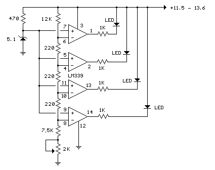 charge condition of a 12 volt, lead acid battery. A 5 volt reference voltage is connected to each of the (+) inputs of the four comparators and the (-) inputs are connected to successive points along a voltage divider. The LEDs will illuminate when the voltage at the negative (-) input exceeds the reference voltage. Calibration can be done by adjusting the 2K potentiometer so that all four LEDs illuminate when the battery voltage is 12.7 volts, indicating full charge with no load on the battery. At 11.7 volts, the LEDs should be off indicating a dead battery. Each LED represents an approximate 25% change in charge condition or 300 millivolts, so that 3 LEDs indicate 75%, 2 LEDs indicate 50%, etc. The actual voltages will depend on temperature conditions and battery type, wet cell, gel cell etc. charge condition of a 12 volt, lead acid battery. A 5 volt reference voltage is connected to each of the (+) inputs of the four comparators and the (-) inputs are connected to successive points along a voltage divider. The LEDs will illuminate when the voltage at the negative (-) input exceeds the reference voltage. Calibration can be done by adjusting the 2K potentiometer so that all four LEDs illuminate when the battery voltage is 12.7 volts, indicating full charge with no load on the battery. At 11.7 volts, the LEDs should be off indicating a dead battery. Each LED represents an approximate 25% change in charge condition or 300 millivolts, so that 3 LEDs indicate 75%, 2 LEDs indicate 50%, etc. The actual voltages will depend on temperature conditions and battery type, wet cell, gel cell etc.
Original scheme edited by Bill
Bowden, http://www.bowdenshobbycircuits.info
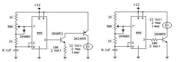
12 Volt Lamp Dimmer
Here is a 12 volt / 2 amp lamp dimmer that can be used to dim a standard 25 watt automobile brake or backup bulb by controlling the duty cycle of a astable 555 timer oscillator. When the wiper of the potentiometer is at the uppermost position, the capacitor will charge quickly through both 1K resistors and the diode, producing a short positive interval and long negative interval which dims the lamp to near darkness. When the potentiometer wiper is at the lowermost position, the capacitor will charge through both 1K resistors and the 50K potentiometer and discharge through the lower 1K resistor, producing a long positive interval and short negative interval which brightens the lamp to near full intensity. The duty cycle of the 200 Hz square wave can be varied from approximately 5% to 95%. The two circuits below illustrate connecting the lamp to either the positive or negative side of the supply.
Original scheme edited by Bill
Bowden, http://www.bowdenshobbycircuits.info
Triangle and Squarewave Generator
Here is a simple triangle/squarewave generator using a common 1458 dual op-amp that can be used from very low frequencies to about 10 Khz. The time interval for one half cycle is about R*C and the outputs will supply about 10 milliamps of current. Triangle amplitude can be altered by adjusting the 47K resistor, and waveform offset can be removed by adding a capacitor in series with the output.
Original scheme edited by Bill
Bowden, http://www.bowdenshobbycircuits.info

Low Frequency Sinewave Generators
The two circuits below illustrate generating low frequency sinewaves by shifting the phase of the signal through an RC network so that oscillation occurs where the total phase shift is 360 degrees. The transistor circuit on the right produces a reasonable sinewave at the collector of the 3904 which is buffered by the JFET to yield a low impedance output. The circuit gain is critical for low distortion and you may need to adjust the 500 ohm resistor to achieve a stable waveform with minimum distortion. The transistor circuit is not recommended for practical applications due to the critical adjustments needed.
The op-amp based phase shift oscillator is much more stable than the single transistor version since the gain can be set higher than needed to sustain oscillation and the output is taken from the RC network which filters out most of the harmonic distortion. The sinewave output from the RC network is buffered and the amplitude restored by the second (top) op-amp which has gain of around 28dB. Frequency is around 600 Hz for RC values shown (7.5K and 0.1uF) and can be reduced by proportionally increasing the network resistors (7.5K). The 7.5K value at pin 2 of the op-amp controls the oscillator circuit gain and is selected so that the output at pin 1 is slightly clipped at the positive and negative peaks. The sinewave output at pin 7 is about 5 volts p-p using a 12 volt supply and appears very clean on a scope since the RC network filters out most all distortion occurring at pin 1.
Original scheme edited by Bill
Bowden, http://www.bowdenshobbycircuits.info

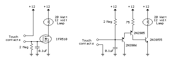
Touch Activated Light
The circuits below light a 20 watt lamp when the contacts are touched and the skin resistance is about 2 Megs or less. The circuit on the left uses a power MOSFET which turns on when the voltage between the source and gate is around 6 volts. The gate of the MOSFET draws no current so the voltage on the gate will be half the supply voltage or 6 volts when the resistance across the touch contacts is equal to the fixed resistance (2 Megs) between the source and gate.
The circuit on the right uses three bipolar transistors to accomplish the same result with the touch contact referenced to the negative or ground end of the supply. Since the base of a bipolar transistor draws current and the current gain is usually less than 200, three transistors are needed to raise the microamp current level through the touch contacts to a couple amps needed by the light. For additional current, the lamp could be replaced with a 12 volt relay and diode across the coil.
Original scheme edited by Bill
Bowden, http://www.bowdenshobbycircuits.info
Neon desktop lamp
This circuit will power a 6 inch 4 Watt fluorescent tube off a 12 volt supply, consuming 300 mA. It may also be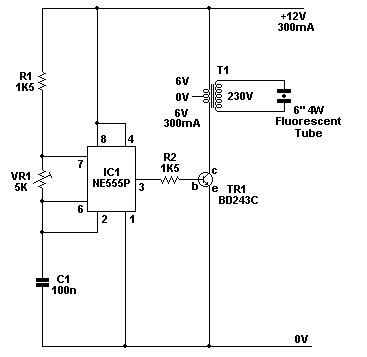 powered by a suitably rated universal AC/DC adapter. Advantages of the design are: good light, low power consumption, and readily available stock parts. The circuit is based on IC1, which is a 555 timer IC in astable mode. IC1's current output is amplified by TR1, and the voltage at the collector is stepped up by T1, a mains to 6-0-6 V transformer. Heat-sinks are advised for TR1 and T1. Before applying power, VR1 should be advanced to a full 5 K. While power consumption is monitored with a multimeter, VR1 should be turned back slowly until power consumption rises to 300 mA maximum. The fluorescent tube should now shine brightly. Power consumption should not exceed 300 mA, or the circuit may be destroyed. Should a universal AC/DC adapter be used at a later stage, constructors are advised to repeat the setup procedure with VR1, since the voltage of such adapters is unstable and may destroy the circuit. Constructors should be aware that a high voltage is present at the transformer primary, which could deliver a nasty shock. powered by a suitably rated universal AC/DC adapter. Advantages of the design are: good light, low power consumption, and readily available stock parts. The circuit is based on IC1, which is a 555 timer IC in astable mode. IC1's current output is amplified by TR1, and the voltage at the collector is stepped up by T1, a mains to 6-0-6 V transformer. Heat-sinks are advised for TR1 and T1. Before applying power, VR1 should be advanced to a full 5 K. While power consumption is monitored with a multimeter, VR1 should be turned back slowly until power consumption rises to 300 mA maximum. The fluorescent tube should now shine brightly. Power consumption should not exceed 300 mA, or the circuit may be destroyed. Should a universal AC/DC adapter be used at a later stage, constructors are advised to repeat the setup procedure with VR1, since the voltage of such adapters is unstable and may destroy the circuit. Constructors should be aware that a high voltage is present at the transformer primary, which could deliver a nasty shock.
Simple microphone preamplifier
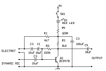 This is a simple microphone preamplifer circuit which you can use between your microphone and stereo amplifier. This circuit amplifier microphone suitable for use with normal home stereo amplifier line/CD/aux/tape inputs. This mic preamp can take both dynamic and electret microphone inputs (preamplifer provides power foe electret microphone elements). The idea of this circuit is to keep the design as simple as possible to be easy to build. That was my goal when I needed a simple external microphone preamplifer for my mixer. The performance of the circuit is nothing superior but can be used with many not so serious projects. The circuit is a simple one transistor amplifier with amplification of about 30-40 dB (depends on transitor, temperature and voltage). The dynamic mic input is just a simple one transistor amplifier circuit with nothing special. Electret microphone input has a resistor R1 fo feeding current through electret microphone capsule when it is connected to the electret microphone input. Electret microphone needs some current (about 1 mA) flowing through it to operate, because there is a small amplifier circuit inside the microphone capsule. This circuit is suitable for all typical cheap electret campsules which available from any electronic component shop. Because electret microphones have higher signal level output, it is quite easy to overdrive the amplifier when you shout to electret microphone. This is a simple microphone preamplifer circuit which you can use between your microphone and stereo amplifier. This circuit amplifier microphone suitable for use with normal home stereo amplifier line/CD/aux/tape inputs. This mic preamp can take both dynamic and electret microphone inputs (preamplifer provides power foe electret microphone elements). The idea of this circuit is to keep the design as simple as possible to be easy to build. That was my goal when I needed a simple external microphone preamplifer for my mixer. The performance of the circuit is nothing superior but can be used with many not so serious projects. The circuit is a simple one transistor amplifier with amplification of about 30-40 dB (depends on transitor, temperature and voltage). The dynamic mic input is just a simple one transistor amplifier circuit with nothing special. Electret microphone input has a resistor R1 fo feeding current through electret microphone capsule when it is connected to the electret microphone input. Electret microphone needs some current (about 1 mA) flowing through it to operate, because there is a small amplifier circuit inside the microphone capsule. This circuit is suitable for all typical cheap electret campsules which available from any electronic component shop. Because electret microphones have higher signal level output, it is quite easy to overdrive the amplifier when you shout to electret microphone.
The circuit is bet to build to a small metal box where you have a small 9V battery for powering it. Battery power and metal box keep noise away.
Ham radio Data Center - free schematics | 73s.eu - Free Ham Radio Social Network | Free HAM Directory | About me | Acronyms | CW | Data Sheets | Docs | Download | E-mail | HOME | Ham projects | Hobby circuits | Photo galery | PIC | QTH photos |
Sign in my guestbook | View my guestbook ]
© 2001 - YO5OFH, Csaba Gajdos |