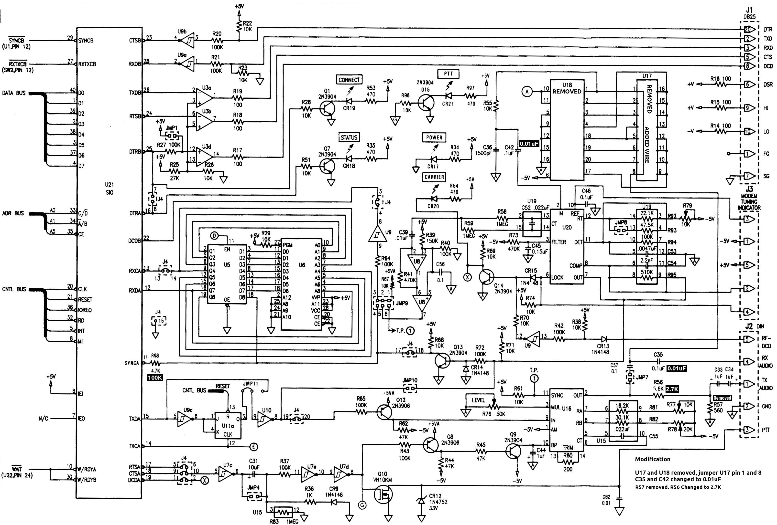
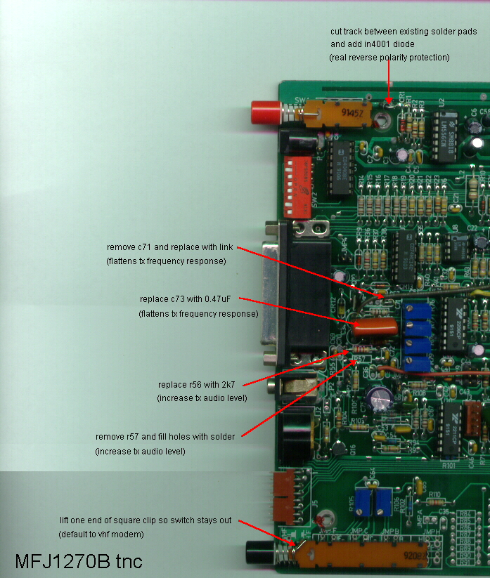
Transmit Level Equalization
These modifications affect only the transmit audio circuitry of the MFJ 1270b and also clean up a few "gotchas" in the use of the tnc.
The main modification is to bring the deviation levels of the low tone and the high tones closer together,
remove the default 6db/octave pre-emphasis implemented in the tnc and increase the tx drive level.
In the unmodified circuit of several MFJ 1270b tested and modified so far, the audio output levels resulted in an
approximate FM deviation of 1.8kHz for the low tone and 4.8kHz for the high tone, the deviation difference being 3kHz.
After modification, the low and high tone transmit audio output levels are such that the FM deviation levels are within 200Hz of each other.
This is particularly critical when connecting to tnc's that use the Exar 2206/2211 chipset for the modem,
(as the MFJ 1270b does) as the demod chip of the set will NOT decode if the recovered low and high tone signal levels are too different.
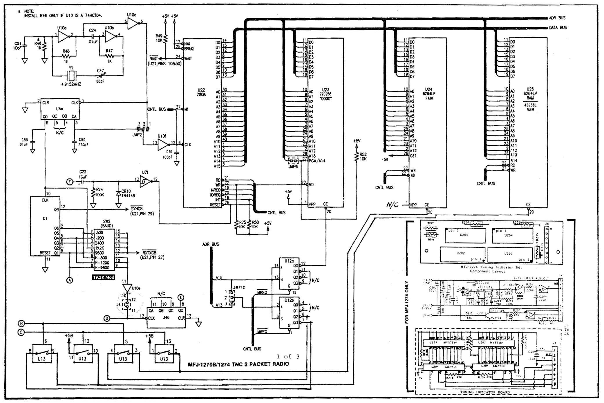
The output circuitry of the MFJ 1270b has two monolithic capacitors in series in the signal path; c71 (4.7nF) which provides 6dB per octave
pre-emphasis (which will add to the 6dB/octave pre-emphasis done in the radio if the tx audio goes through the mic amplifier) and
c73 (0.33uF) which decouples the transmit audio output of the XR2206 modem.
The four components (c71, c73, r56 & r57) of the tx audio path form a filter whose response is frequency dependent.
Changing the capacitor values changes the filter's effect on the low and high tones, changing the resistance values increases the tx audio level.
The output deviation level mod as shown is to short out c71, change r56 (7.5k) to 2.7k, remove r57 (560r) and
change c73 (0.33uF) to 0.47uF. The analogue loopback feature provided by jmp7 is unaffected by this modification.
(NOTE: For the MFJ 1270, just change r56 and remove r57.)
After modification the difference between the low and the high tone deviation levels is approx 200Hz.
[VK3XSW Mods]
Warren Stirling, VK3XSW 13-11-2002
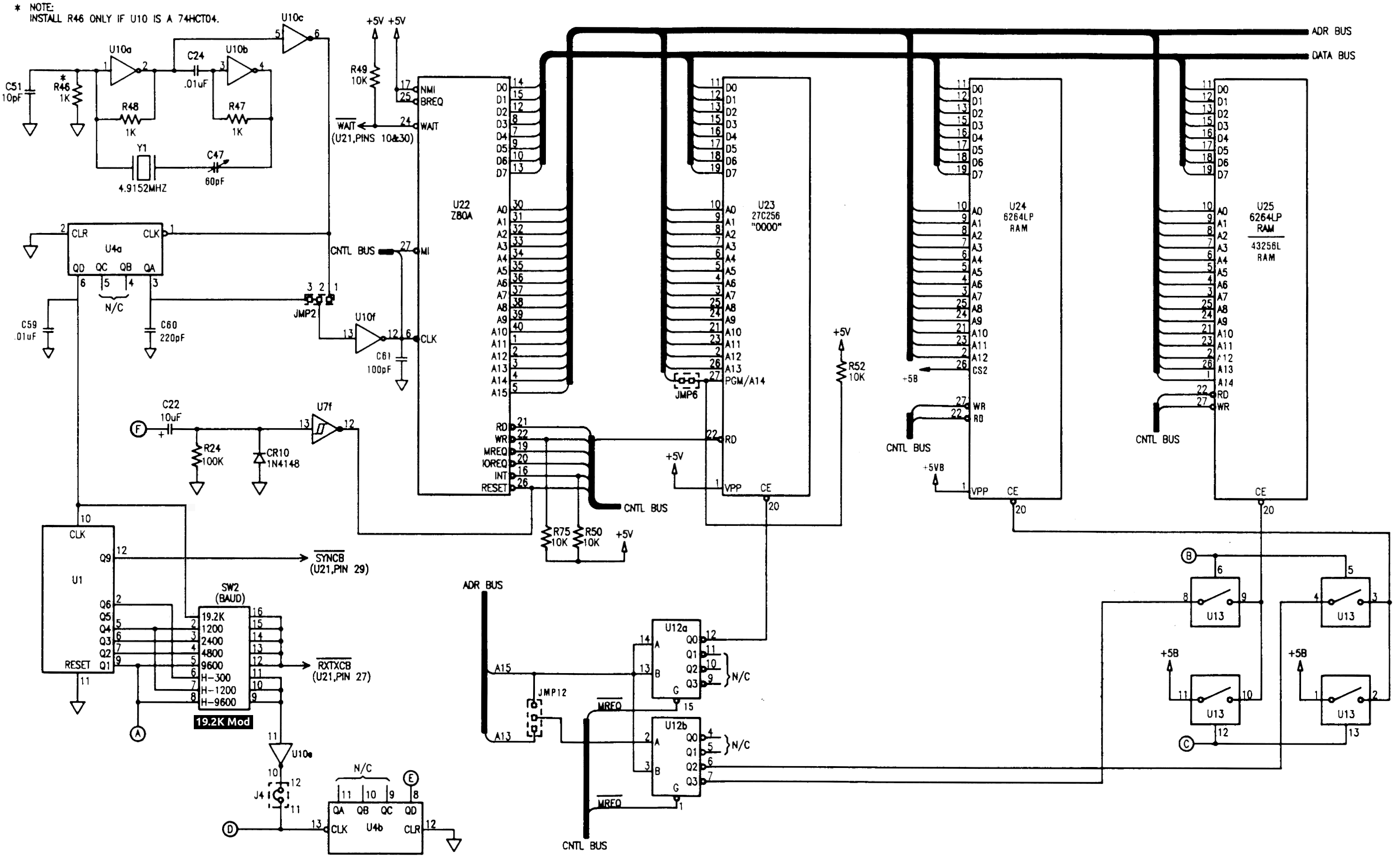
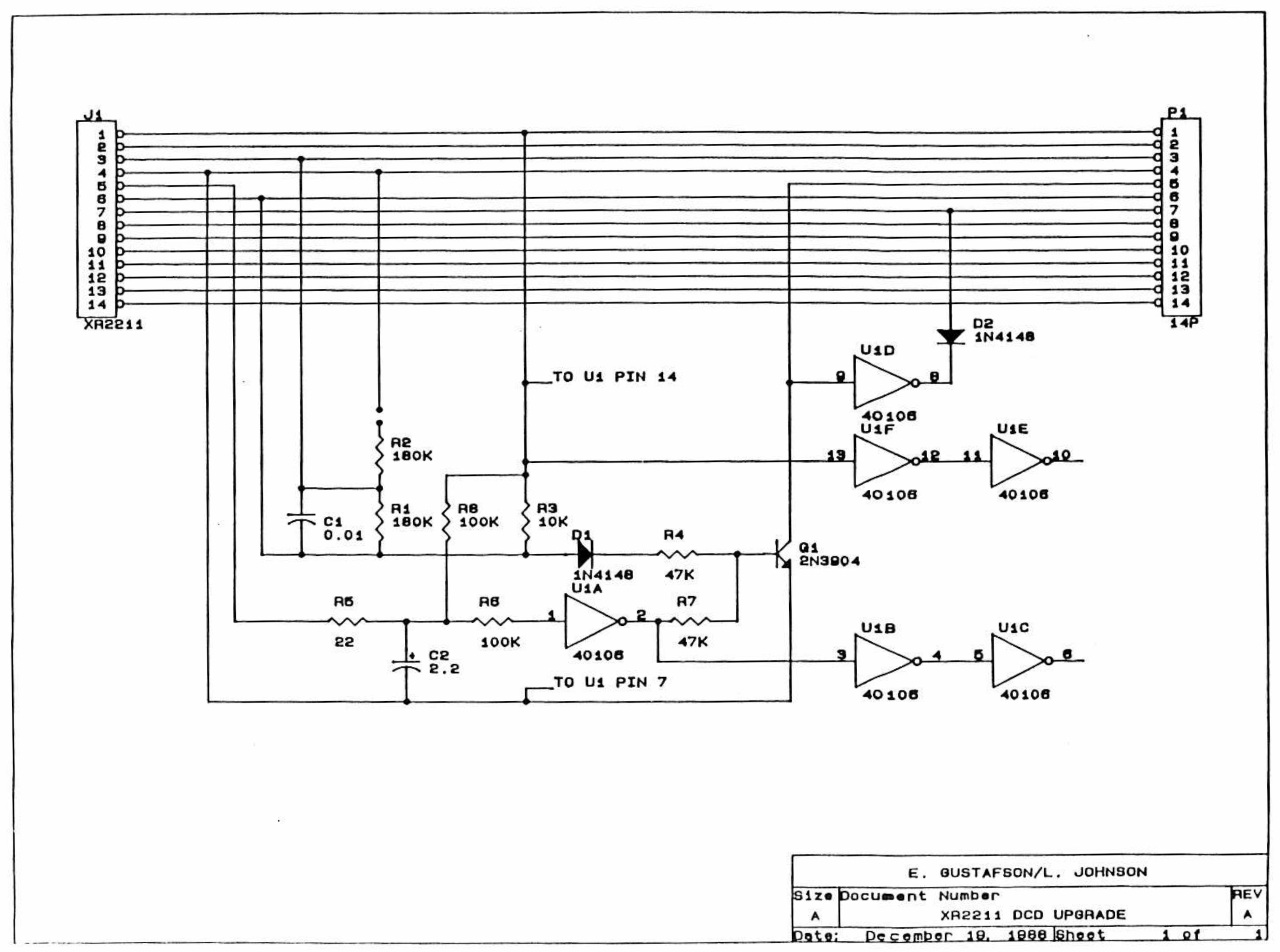
TAPR XR2211 DCD Upgrade
[Schematic]
DCD information from the XR2211 demodulator is
available at pin 6 (positive) and pin 5 (negative), both
of which are open-collector outputs.
Pin 5, which goes to ground when DCD is true,
rapidly discharges C2 through R5. U1A inverts this
information, turning Q1 on via R7. The low state of
the Q1 collector is passed along to the TNC as an
open-collector output of the same polarity as pin 7 XR2211.
The Q1 low state is also inverted through U1D and
reverse-biases D2, removing it from the circuit.
When DCD is no longer valid, C2 charges through
R8, resulting in a "hang" time of a fraction of a second.
The hang time is necessary in the case of multipath
fades, collisions which result in a lack of detectable
information to the XR2211 phase-locked-loop, etc.
After the hang time elapses, U1A goes low, turning
Q1 off. U1D then goes low, pulling the data output
line (pin 7) low through D2. Since pin 7 is an open-
collector output, this eliminates random transitions
on the output from the demodulator.
R1, C1 and R3 provide a fast-attack to the DCD output
by driving Q1 on (via D1 and R4) much faster than
the R5/C2 path. In addition, this network provides
hysteresis to the DCD decision circuitry within the
XR2211 chip. The result is a more positive decision
with less "chattering" in the presence of noise.
Finally, R2 (180K alone or 27K in series with a
THRESHOLD control) balances the currents in the
DCD circuitry of the XR2211 chip to reduce false
decicions. The THRESHOLD control option allows
tailoring the DCD response to the specific filters and
noise levels in effect at a given time.
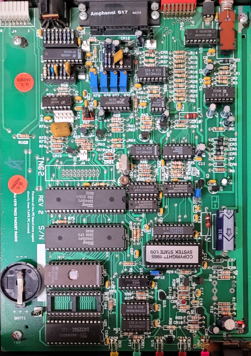
TAPR XR211 DCD Upgrade board layout
.png)


