I personally have designed and built high power class E transmitters for 40, 80 and 160 meters.
Class E transmitters are high efficiency, highly reliable, solid state transmitters. They are simpler to build than similar transmitters using vacuum tubes, and are significantly less expensive to both build and to operate.
This site introduces class E, and explains some of the concepts. For complete information, including schematics and pictures of real, practical transmitters, please to go to: The Official Class E Web Site Please let me know if there are errors or if there is missing information :-)
There are three capacitances at work within the FET itself; the input capacitance, the output capacitance and the so-called "transfer" (drain to gate) capacitance. The effects of the capacitances within the FET are reduced by making the capacitances part of resonant circuits rather than "forcing" energy into and out of the capacitances. Let's look at the various elements.
The element we must consider first, as far as class E operation is concerned is the the drain, or output capacitance. This capacitance exists from drain to source. In normal switching arrangements, this capacitance is simply charged and discharged by the FET(s). However, as the frequency is increased, more and more current is required to quickly charge and discharge this FET capacitance. If this current flows through the FET, the FETs internal resistance will dissipate power. The efficiency will drop dramatically as the frequency is increased. In class E, the output network values are chosen such that the output capacitance is part of a total resonant circuit. The capacitor is "charged" by the flyback effect of the tuned circuit.
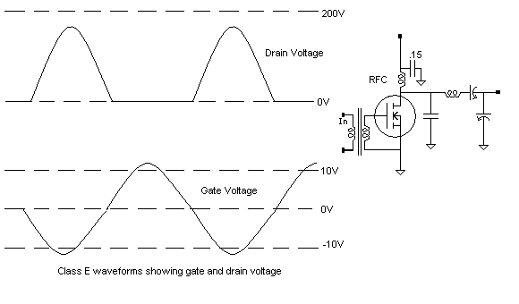
The diagram below shows a basic class E RF ouput stage, and the drain and gate voltage waveforms when properly adjusted. The DC voltage applied to the drain in this example is 50Vdc. Notice the peak RF drain voltage rises to almost 200v.
The the gate, or "input" capacitance will prevent the FET from being driven easily at high frequencies. This capacitance is very high in most FETs - in some cases, in the order of thousands of picofarads for a single FET. Values which we would consider to be a "short circuit" to RF in the vacuum tube world are commonplace operating values in the FET world. The most effective way to deal with the input capacitance is to make it part of a resonant circuit, and drive it with a very low impedance driver. All of the energy which is put into the gate is lost in the form of heat, caused by the charging and discharging of the gate capacitance. It is only necessary to drive the gate to about 10v (positive). The FET will be fully saturated at this point. It is possible to "drive" the FET with a square wave, however as the frequency is increased, the amount of power required to force a square wave into the gate capacitance becomes excessive.
The reverse-transfer capacitance effects the ability of the FET to be driven when high voltage is present at the drain. Ideally, you want to choose a FET which has as low a reverse-transfer (also called the Miller capacitance) capacitance as possible. The reverse-transfer capacitance causes the drain voltage to "work against" the gate voltage. Improvements in technology and manufacturing techniques have dramatically reduced reverse transfer capacitances over the past few years. Be aware of this value, along with the related Gate Charge value when choosing FETs for RF applications. The lower the gate charge, the better is the FET for RF.
This site introduces class E, and explains some of the concepts. For complete information, including schematics and pictures of real, practical transmitters, please to go to: The Official Class E Web Site