Original design: Dallas Lankford - 15 NOV 1991
Article & modified version: Mark Connelly - 04 FEB 1992; converted to HTML 15 JUN 2001
The BFE-C (Balanced Front-End Card, model C) is a "WA1ION DX Labs" implementation of Dallas Lankford's Balanced Cascode Loop Amplifier. Dallas's design differs slightly from BFE-C in minor ways that will be mentioned subsequently.
In terms of electrical characteristics, both can be treated as the same entity. The design is an improvement on the Kolb-Sanserino amplifier long used in Radio West's loops as well as (in modified form) in the RTL-1 Remotely-Tuned Loop (BFE-A, BFE-B cards). Dallas maintains that the balanced configuration of the output transistors (Q3 and Q4) of the new design improves noise figure; using FET's in the output stage, rather than a bipolar transistor gives enhanced strong-signal performance (i. e. reduced spurious responses).
This article will not go into an in-depth design review. Dallas's articles can be obtained from the National Radio Club's reprints service. The essential construction details will be supplied, so DXers can do testing of their own.
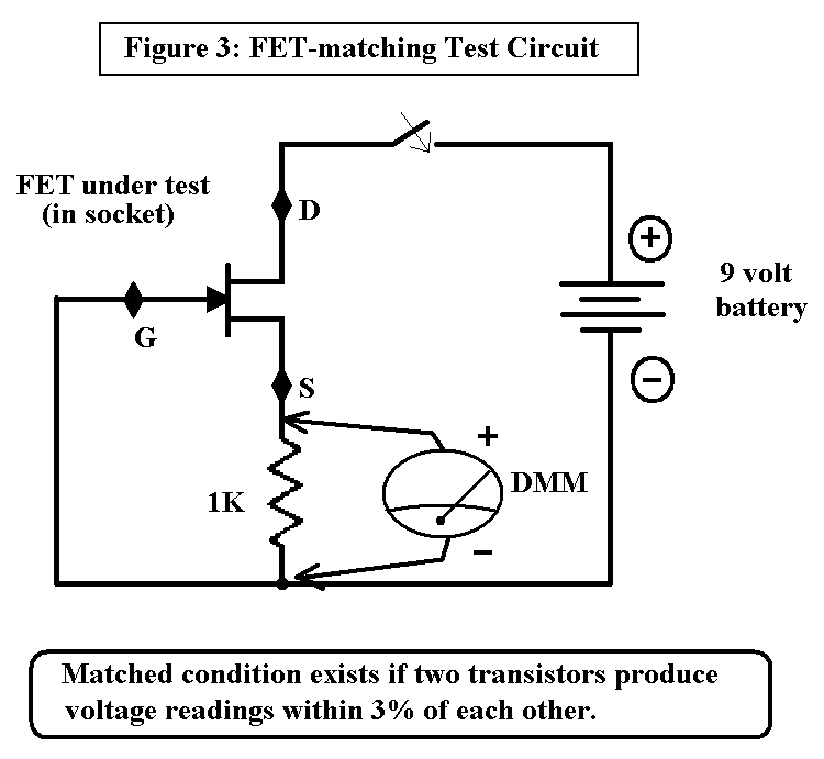
Figure 1 is the BFE-C schematic, Figure 2 is its assembly (component layout) drawing, and Table 1 is the parts list. For best results, Q1 should be matched to Q2; also, Q3 should be matched to Q4. Figure 3 shows the test circuit for measuring the voltage used to ascertain a matched condition. Two transistors producing voltage readings within 3% or better can be considered to be matched. For the purpose of getting two matched pairs of MPF102's, you should have a dozen or so transistors available.
Dallas Lankford suggests using an Amidon ferrite bead (part number FB-101-64) on the drain lead of Q1 and one on the drain lead of Q2 rather than using low-value chokes L3 and L4. The 100 uH input inductors L1 and L2, meant to reduce sensitivity above 9 MHz, can be removed if the loop amplifier is to be used with a shortwave, rather than with a medium wave, loop. R3 and R4 may each be reduced to 2.2K or to an even lower value. This will reduce gain, thereby reducing spurious responses that can occur in urban areas with large air-core loops. With lower-gain ferrite loops, it is unlikely that overloading would be much of a problem except in the worst "transmitter alley" locations like the New Jersey Meadowlands. Dallas has recommended that larger loops be tapped down part way on the coil - again to improve dynamic range and to reduce intermodulation distortion "spurs" in strong-signal areas. He also mentioned problems with Mouser inductors opening up (a problem I've seldom encountered); he winds homebrew 100 uH inductors using 39 turns of #26 wire on an Amidon FT-50-82 toroidal core. He also homebrews the output balun transformer (12 trifilar turns #22 on Amidon FT-82-43, or 33 trifilar turns #26 on Amidon FT-82-61). There doesn't seem to be a parametric advantage to one approach (e. g. homebrew) over the other (e. g. using the Mini-Circuits T4-6T).
Table 1: (A1) BFE-C balanced front-end card parts list
Vendor codes:
DK = Digi-Key = http://www.digikey.com
MCL = Mini-Circuits = http://www.minicircuits.com
MOU = Mouser Electronics = http://www.mouser.com
RS = Radio Shack = http://www.radioshack.com
|
Item |
Designator |
Description/Value |
Vendor |
Vendor Stock # |
QTY |
1 | BD | perfboard(1.9"X1.4") | RS | 276-1396 (cut) | 1 |
2 | C1-C4 | capacitor, 0.1 uF | DK | P4525 | 4 |
3 | H1-H4 | screw, 4-40 X .25" | MOU | 572-01880 | 4 |
4 | H1-H4 | spacer, 4-40 X .5" | MOU | 534-1450C | 4 |
5 | H1-H3 | split lockwasher, #4 | MOU | 572-00649 | 4 |
6 | H4 | solder lug, #4 | MOU | 534-7311 | 1 |
7 | L1-L2 | inductor, 100 uH | MOU | 43LS104 | 2 |
8 | L3-L4 | inductor, 1 uH | MOU | 43LS106 | 2 |
9 | P1-P19 | flea-clip, .042" hole | DK | V1069-ND | 19 |
10 | Q1-Q4 | FET, MPF102 | RS | 276-2062 (see note) | 4 |
11 | R1 | resistor, 1K | RS | 271-1321 | 1 |
12 | R2 | resistor, 47 ohm | MOU | 29SJ500-47 | 1 |
13 | R3-R4 | resistor, 4.75K,1% | DK | 4.75KX | 2 |
14 | R5-R6 | resistor, 2.21K,1% | DK | 2.21KX | 2 |
15 | T1 | 4:1 RF transformer | MCL | T4-6T-X65 | 1 |
16 | W | buss wire | RS | 278-1341 | ~1' |
Note: Q1 and Q2 should be matched. Q3 and Q4 should be matched. FET-matching method is shown in Figure 3.
Figure 1: BFE-C Schematic
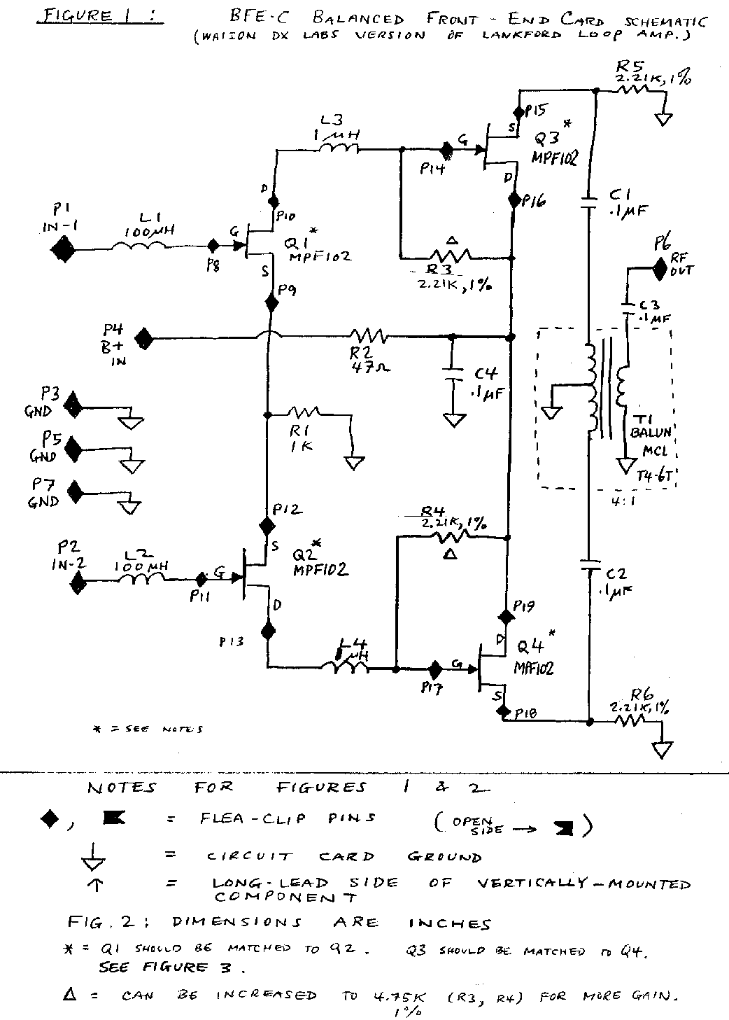
Figure 2: BFE-C Assembly
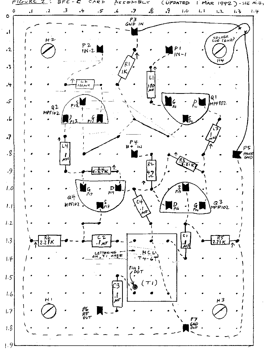
Figure 3: FET Matching Circuit