PCBs, Kits & Assembled Units are Available NOW!
Dealers & Stockists Required Outside INDIA. Please Contact.
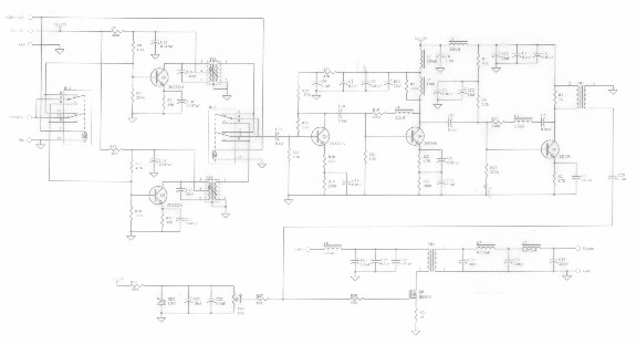
Download Transmitter Schematic Diagram
This is the actual power generation section of the transceiver. The output from the Transmit Mixer section of the Receiver PCB is slightly amplified (using a single stage 2N2222 amplifier) & filtered through a Band Pass Filter TR2 or TR3. TR2 consists of 10 turns Bifilar winding in the Primary and 5 turns single winding in the Secondary. TR3 has 6 turns Bifilar winding in the Primary and 5 turns single winding in the Secondary. Both are wound with 36SWG enameled copper wire. This TX signal is then amplified to the desired power output levels in three stages. The first stage consists of a 2N3866 amplifier that increases the power level to about 250mW. This is again amplified to about 1watt by a BD139 transistor & TR1 consisting of 6 turns in the Primary and 4 turns in the Secondary, wound with 28SWG enameled copper wire.
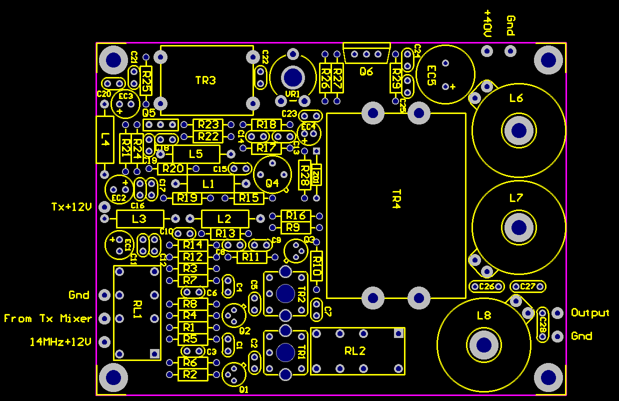
Download Transmitter Layout Diagram
The BD139 output is used as driver stage for the IRF510 Power Amplifier. The IRF510 is a rugged device that can withstand heat and SWR fluctuations. With a regular 12V DC supply, the power output is around 4 to 5 Watts and is enough for QRP (low power) operation. However, with a 36V DC supply, the IRF510 with the same settings & component combination will deliver around 25Watts RF power which is good enough for a comfortable DX chat. IRF510 output is tuned to the desired frequency & power output level by TR4 consisting of 6 turns in the Primary and 8 turns in the Secondary wound with 18SWG enameled copper wire. This is further filtered, to kill any unwanted harmonics, by a Low Pass Filter made of L6, L7, C26, C27 & C28.

Download TX PCB Image
Download Bill of Materials text file for the TX PCB
You are visitor number
Return to Home Page
Email: Jagdish, VU2JH