 |
INTRODUCTION
A low distortion audio frequency sine wave can be easily generated by passing the output of a simple square wave oscillator through a sharp cut off low pass filter to attenuate the odd harmonic components. The output level of the sine wave is precisely defined by the rail voltage and the gain or loss in the filter.
A problem is that most filters have a fixed cut off frequency hence such a sine wave source is restricted to a small frequency range. There is, however, one type of integrated circuit package containing a switched capacitor fitter in which the cut off frequency can be controlled by the frequency of a clock running at a multiple of the cut off frequency. The circuit described in this article makes use of a switched capacitor low pass filter type MF6-50 (a sixth order Butterworth) which operates with a clock frequency 50 times its cut off frequency. By controlling the frequency of the clock, the cut off frequency can be set to a range of values extending to above 20 kHz.
Using this filter, the circuit forms a variable frequency sine wave oscillator which can be tuned, at constant output level, over a frequency range of 2 Hz to 20 kHz with harmonic components less than 0.1 percent of the fundamental frequency amplitude, that is, more than 60 dB below that amplitude. As the sine wave is formed from a square wave, the square wave is also available as an alternative output.
THE SYSTEM
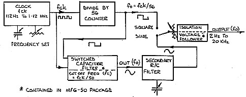
The basis of the system is shown in the block diagram, Figure 1. A clock (fck), tunable within the range of 112 Hz to 1.12 MHz drives both the switched capacitor fitter and a divide by 56 counter which gives square wave output in the range of 2 Hz to 20 kHz. The counter output is fed to the input of the filter which has a cut off' frequency (fc) equal to fck divided by 50, that is, 12 percent higher than the output frequency of the counter. With this arrangement, odd order harmonics in the square wave are attenuated to a level less than 60 dB below the fundamental frequency. Whatever the fundamental frequency, the cut off frequency tracks at 12 percent higher because both are controlled by the same clock source.
|
|
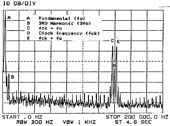
A characteristic of the filter is that it produces components near clock frequency 34 dB down from the fundamental frequency. These can be clearly seen on the CRO display and the spectrum plot of the filter output illustrated in Figure 2. The actual components are the clock frequency itself plus difference components between the clock frequency and the fundamental frequency. For general audio frequency testing, these components, around 56 times the operating frequency, are possibly unlikely to upset the results of the testing. Notwithstanding this, their presence is a little disconcerting hence a simple secondary R-C filter is included, at the output of the switched capacitor filter, to reduce their level.
|
 |
THE CIRCUIT
The complete circuit is shown in Figure 3. In addition to the switched capacitor filter, the MF6-50 package includes circuitry which can be connected up to form the clock by the addition of an external resistance-capacitance network which determines the frequency of oscillation. A frequency range of 112 Hz to 1.12 MHz can easily be covered with four ranges of selected capacity using a 40 kohm potentiometer, however it was found that eight ranges using a 25 kohm potentiometer was more satisfactory, firstly because of the improved resolution in setting a given frequency and secondly because of a problem in making the secondary R-C filter effective over too wide a range. The clock R-C network in Figure 3 is made up of R4, RV1 and C3A-H.

The secondary R-C filter is provided by resistor R6 and capacitors C6A-H switched in tandem with those selected for clock frequency range. The circuit reduces the high frequency ripple component to 55 dB below the operating frequency level at the high frequency end of the selected range (refer to Figure 4) and 45 dB below at the low frequency end (refer Figure 5). At 45 dB down, the ripple can just be seen on the CRO trace.

|
 |

|
 |
Capacitor values of C3 and C6 switched in for the the various frequency ranges are given in the following table:
| RANGE | FREQ | C3 | C6 |
| 1 | 2 - 6.3 Hz | 200 nF | 1.2 uF |
| 2 | 6.3 - 20 Hz | 62nF | 390.0 nF |
| 3 | 20 - 63 Hz | 20nF | 120.0 nF |
| 4 | 63 - 200 Hz | 6.2 nF | 39.0 nF |
| 5 | 200 - 630 Hz | 2nF | 12.0 nF |
| 6 | 630 Hz - 2 kHz | 510 pF | 3.9 nF |
| 7 | 2 - 6.3 kHz | 130 pF | 3.0 nF | |
| 8 | 6.3 - 20 kHz| 27 pF | 1.5 nF | |
Included in the MF6-60 package are two operational amplifiers. One of these is used as a source follower stage to isolate the secondary filter and output level control from the output circuit as well as providing low source resistance at the output. A transistor (V1) is included in the operational amplifier loop to provide sufficient current drive for the amplifier to operate as a 50 ohm source. Output of the stage is directly coupled to eliminate the very large coupling capacitor needed to prevent excessive waveform drop on 2 Hz square wave. Output resistance is set to 50 ohms by resistor R8.
A switch is provided so that either sine wave or square wave can be selected. The sine wave circuit is coupled via capacitor C7, found necessary because the output of the switched capacity filter had a DC offset.
The 4520B package contains two four-stage counters connected to divide by seven and eight respectively. The divide by seven counter must not be placed last because a divide by seven counter has an asymmetrical output waveform. The high speed CMOS version of the 4520 was used to ensure short rise time in the square wave output.
Provision of a split power rail (dual five volts) simplifies the application of direct coupling used throughout the circuit. The supply must be regulated as both clock frequency and output amplitude vary with rail voltage.
PERFORMANCE
Figure 6 is a spectrum plot showing the level of harmonics in the output. The highest level component is the third harmonic at 62 dB down and other odd order harmonics are more than 80 dB down. The second order component, 65 dB down, is not actually a harmonic originating from the square wave at the input to the filter. It is caused by interference from the second to last stage of the counter running at the second order frequency.
 |
Examining the circuit (Figure 3), large capacitors are connected across the rails to ground at both circuit packages. These are essential to reduce interference from the counter and are quite large because of the very low frequency ranges covered by the oscillator.
The capacitor values in the secondary filter have been carefully selected to reduce the high frequency ripple as much as possible without upsetting the consistency of output voltage over the tuning range. An increase in capacitance value can reduce the ripple further but would cause a reduction in output level as the high frequency end of each range is approached.
On the highest frequency range, the switched capacitor filter produced an increase in output level towards the high frequency end of the range. The reason for this was not clear but its effect was compensated by increasing the secondary filter capacitor to a higher order than the other ranges. In consequence, the ripple level on this range is lower than on the other ranges.
Maximum output level for both sine wave and square wave is 1.5 VPP when unloaded or half that with 50 ohms load. DC load current on the five volt rails is 28 mA, mainly consumed by the output transistor.
ASSEMBLY CONSIDERATIONS
With the clock operating to a frequency above 1 MHz, at a voltage level of 10 VPP inappropriate layout and proximity of wiring can lead to coupling of clock frequency component into sections of the output circuit. In the experimental model built, it was found necessary to shield all wiring following the switched capacitor filter output to reduce stray coupling into the output circuit when operating on the two highest frequency ranges.
Range selection capacitors were mounted around the switch wafers rather than on the component mounting card. This eliminated the need for a large number of wires between the switch banks and the card. The values of capacitors (C3A-H) which set the clock frequency are shown in Figure 3 and in the table, as nominal values. In the experimental model, ordinary 10 percent ceramic capacitors were used and trimmed by experiment using large and small values in parallel to make the frequency ranges overlap.
CONCLUSION
The circuit described is an interesting alternative to the conventional Wien Bridqe oscillator which requires a ganged variable tuning capacitor and feedback to stabilise the output level. A criticism could be the ripple level near clock frequency 45 to 55 dB down. The level of this is determined by the secondary filter and could be improved with a more complex filter circuit than the simple one used.