Today the "Software Defined Radios - SDR" gain more and more followers, but in the same time many radio home-brewers still get a lot of fun and satisfaction building old style "Hardware Defined Radios".
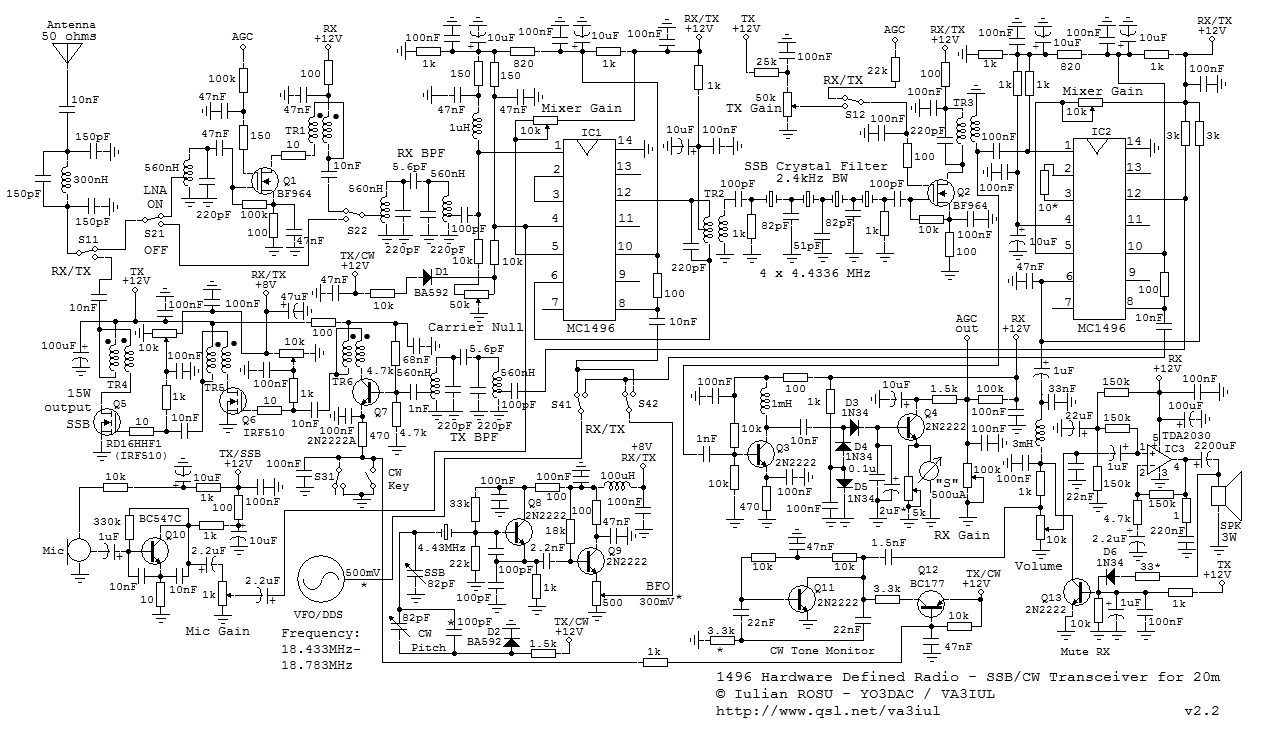
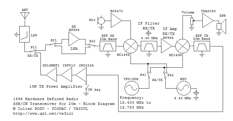
This compact and inexpensive SSB transceiver presented here is based on two MC1496 integrated circuits.
MC1496 was developed by Motorola and released to the market in 1972. Since then the license to produce the circuit was given to many other chip manufacturers (Philips, Signetics, JRC, ON Semi, etc).
In the history of semiconductors there are very few integrated circuits that are still in production after more than 40 years from their initial release. MC1496 is one of them. ON Semi and JRC they are still producing the chip, with a market price less than $1. You can buy MC1496 from here or from here.
People might say that a disadvantage of MC1496 is it's high count of external bias resistors, compared to newer similar chipsets (e.g. SA612, MC13143, uPC1037, NJM2594, etc.) which uses internal bias resistors.
This disadvantage actually could be a benefit if the designer wants to adjust the bias current of the mixer (or modulator/demodulator), improving in this way some characteristics as: gain, intermods, or the noise figure.
MC1496 provides an external Carrier Null circuit, getting better carrier rejection than other similar circuits, where the balance is done inside of the chip.
Even if the dual supply voltage (+12V and -8V) is recommended in the MC1496 datasheet, this is not mandatory to be used, and the chip works fine with a single +12V power supply. But supplying MC1496 with dual (+/-) supply voltage improves the linearity (intermods), the gain, and carrier suppression as well. I found that supplying the entire transceiver with single +13.8V (instead of single +12V) most of the performances (RX and TX) improves. This is an option for every builder, to what voltages have available. In this radio only the oscillators (VFO and BFO) are supplied from a +8V regulator.
Because the MC1496 is a transformer-less circuit (Gilbert cell), theoretically this have no limit in low frequency characteristic (as ring diode mixers which use transformers), and the useful working frequency can be practically down to the DC. When the circuit is used as a DSB (Double Side Band) modulator the rejection of the carrier is better than 55dB when use single DC supply.
On the RX front-end side, the transceiver use a switchable ON/OFF LNA (Q1) which can be any low noise dual-gate MOSFET (BF964, BF981, BF960, BF998, BF901, etc). The signal is passed further to the receive down-conversion mixer (IC1) which is based on MC1496. The same circuit is also used by the transmitter as a balanced DSB modulator (Double Side Band, Suppressed-Carrier). The received RF signal (14MHz) and the transmitter audio signal from the microphone use separate inputs of the MC1496 (IC1). To get maximum conversion gain and sensitivity the external emitter resistance on the lower differential amplifier pair has been reduced to zero (short between pin 2 and 3 of MC1496).
In CW TX mode the balanced DSB modulator is DC off-set to an unbalanced mode, canceling in this way the "Carrier Null" circuit. The DC offset is done using a 10K resistor connected to Vcc through a switching diode (D1).
The VFO (~18.433 MHz) in RX mode, and the BFO (4.43 MHz) in TX mode, use the same input (pin nr. 8 of IC1) in both modes, RX and TX . The output of the IC1 (MC1496) is a transformer resonator (TR2) tuned on 4.43 MHz, and used by both modes, RX and TX.
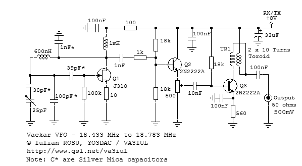
For 20m band, when using 4.43 MHz as intermediate frequency (IF), and high-side LO injection, the frequency of the VFO has a frequency range from: 18.433 MHz to 18.783 MHz.
The VFO its a Vackar FET oscillator, which is a pretty stable oscillator. This oscillator can be used initially only to power-up and to tune the radio, and later to be replaced by a DDS VFO.
For less than $20 you can build a DDS VFO with direct frequency reading based on AD9850 chipset, if you buy the components from here: DDS module, Arduino Nano module, LCD Display, Rotary Encoder.
The schematic of the DDS VFO, code and libraries, and any other information you can get from AD7C website. This useful DDS VFO have the ability to combine the VFO and IF frequencies and to show on the LCD display exactly the received RF frequency.
The Crystal Ladder Filter uses four identical 4.4336 MHz Crystals (PAL sub-carrier). I have made this transceiver with different intermediate frequencies using crystals at 8.86 MHz, 9 MHz, 10MHz, and 10.7 MHz, also in ladder configuration. For amateur test conditions I found that the 4.43 MHz Intermediate Frequency is the most suitable option when using only four stock crystals. The Intermediate Frequency placed on 4.43 MHz also gives lower VFO frequency, when use high-side LO injection. High-side LO injection is necessary in the receiver to move up in frequency the image frequency, making easier its rejection. The image frequency in our case is about 23 MHz, almost 9 MHz far from the receive frequency.
Notice About Ladder Crystal Filters
The measured bandwidth and out-of-band rejection of ladder crystal filters have a limit of using up to 6 crystals.
Increasing more than 6 the number of
crystals, the performances of the filter increase insignificantly.
Compared to bridge/lattice filter types, ladder crystal filters have the
advantages enumerated below:
- All crystals are of the same frequency and no matching, grinding or etching is
required.
- Spurious responses are not so detrimental to overall performance of the filter
and, for filters having more than 4 sections, may be virtually undetectable.
- Filters may be constructed using an odd or even number of crystals. This is a
useful attribute when one is dependent upon surplus sources for the supply of
crystals.
- The only other components required are the 2% (approximately) tolerance
capacitors (preferable high quality silver-mica) and the preset trimmers (if are
required).
- Because of the very low equivalent series resistance of crystals, the
insertion loss of these filters is very low.
The IF amplifier transistor (Q2) could be any low noise dual-gate MOSFET (BF964, BF981, BF960, BF998, BF901, etc). This stage is used in both modes, RX and TX. In receive mode the gate number two (G2) of the MOSFET is controlled by the AGC, and in TX mode it's controlled by the TX gain potentiometer. Both potentiometers (TX gain and RX gain), should be placed on the front panel of the transceiver, together with the audio volume potentiometer.
The receive AGC circuit has an IF amplifier (Q3), a Germanium diode detector (DC biased), and a drive amplifier (Q4) which has the "Strength-meter" in the emitter.
The second MC1496 (IC2) is used in receive mode as a Product Detector, and as an up-conversion RF mixer in transmitter mode. The two outputs of the IC2 are used simultaneous between RX/TX modes (no switch need). Pin 6 is for audio output, and pin 12 is for TX RF output.
The levels of the two switched oscillators (VFO and BFO) on the IC2 are the same as in IC1 case (pin 8 of MC1496). Operating with a high carrier level input maximize the device gain and insure that any amplitude variations present on the carrier do not appear on the output sidebands. It has the disadvantage of increasing some of the spurious signals and lower carrier rejection.
Another benefit of the MC1496 working as a Product Detector is its high sensitivity. At frequency of 4.43 MHz the input sensitivity (only of the Product Detector) is about 3uV for a 10dB Signal plus Noise over Noise [(S + N)/N] ratio, which is fine for receiving an SSB signal. The gain of the mixer in those conditions is about 12dB, and the audio output level is enough to drive directly the TDA2030 audio power amplifier.
The total sensitivity of the receiver is better than 0.2uV with the LNA switched ON. As a result of high sensitivity of the Product Detector, the gain of the receiver from antenna connector to the detector input, is not necessary to be very high, improving in this way the overall receiver linearity and noise floor.
As a remark, some home-brew circuits using MC1496 fail the performances for a simple reason, because they don't use a variable resistor to adjust the gain of the integrated circuit (resistor connected from pin nr. 5 to Vcc when use single supply, or connected to the ground when using dual +/- supply). The adjustment of this resistor is critical for various bias currents and Vcc voltages of MC1496.
The output of the TX RF mixer (pin 12 of IC2) is relative high level, and using after the mixer only three amplifier stages you can get about 15W output power at the antenna connector. The first TX amplifier placed after the TX BPF (Band Pass Filter) is using a 2N2222A, transistor which is driving an IRF510 MOSFET, which further is driving the final stage. The final stage use a 16W Mitsubishi transistor RD16HHF1. You can buy RD16HHF1, toroids, IF inductors, Silver Mica capacitors, and other components from here. At the cost of loosing some of the PA linearity and output power, the transistor RD16HHF1 can be replaced with a cheap IRF510 (same as the driver transistor). In this case, the total output power will be less than 10W.
Tuning of the transceiver is relative simple. May start tuning the transmitter injecting an audio signal (ideally dual-tones) at the microphone input, and tune the following resonant circuits for maximum output power at antenna connector: TR2, TR3, and TX BPF. In TX mode also adjust the two Mixer Gain resistors, the TX Gain variable resistor, and the quiescent current of the RF power MOSFET transistors. Both TR2 and TR3 resonates on 4.43 MHz and they are also used by the receiver, so their tuning point should be the same in both modes.
For adjusting the carrier rejection need an oscilloscope probe placed before the Crystal Filter, and adjust for minimum carrier leakage from the "Carrier Null" variable resistor. The nulling circuit permits minimizing of the LO signal and results in a few dB additional LO suppression at the mixer output (LO-to-IF rejection). The symmetry of the LO signal is important to get good carrier suppression. Compared to a sine wave LO signal, a square wave LO signal with 50% duty cycle can give up to 15dB more carrier rejection.
The BFO frequency should be about 1.7kHz from the central frequency of the Crystal Filter. The 82pf (SSB) trimmer capacitor in series with the crystal of the BFO will be adjusted in this regards.
In CW mode the frequency of the BFO (and the CW pitch) is set by a group of capacitors placed in parallel with this trimmer capacitor using a switching diode circuit (D2).
In receive mode, injecting a low level RF signal at antenna input, tune first the RX BPF resonators with LNA switched OFF. After that switch the LNA ON, and tune the LNA input resonator. Mixer Gain resistors should be adjusted in RX mode also, and there might be a small compromise between TX and RX modes.
The four pairs of switches in the schematic (S11-S12, S21-S22, S31-S32, S41-S42) are low power Signal Relays. On the schematic the switches are shown in RX mode position, and the LNA is shown in ON position.
In CW TX mode the CW key is switching the emitter of Q7. In parallel with the CW key there is the S32 switch, which is in closed position in SSB TX mode.
The CW Tone Monitor circuit is done using Q11 and Q12 transistors. The frequency of the audio tone could be adjusted varying the 3.3k* resistor.
The audio power amplifier is based on TDA2030, circuit which was presented in earlier schematics as a good choice for a low distortion and low noise audio amplifier.
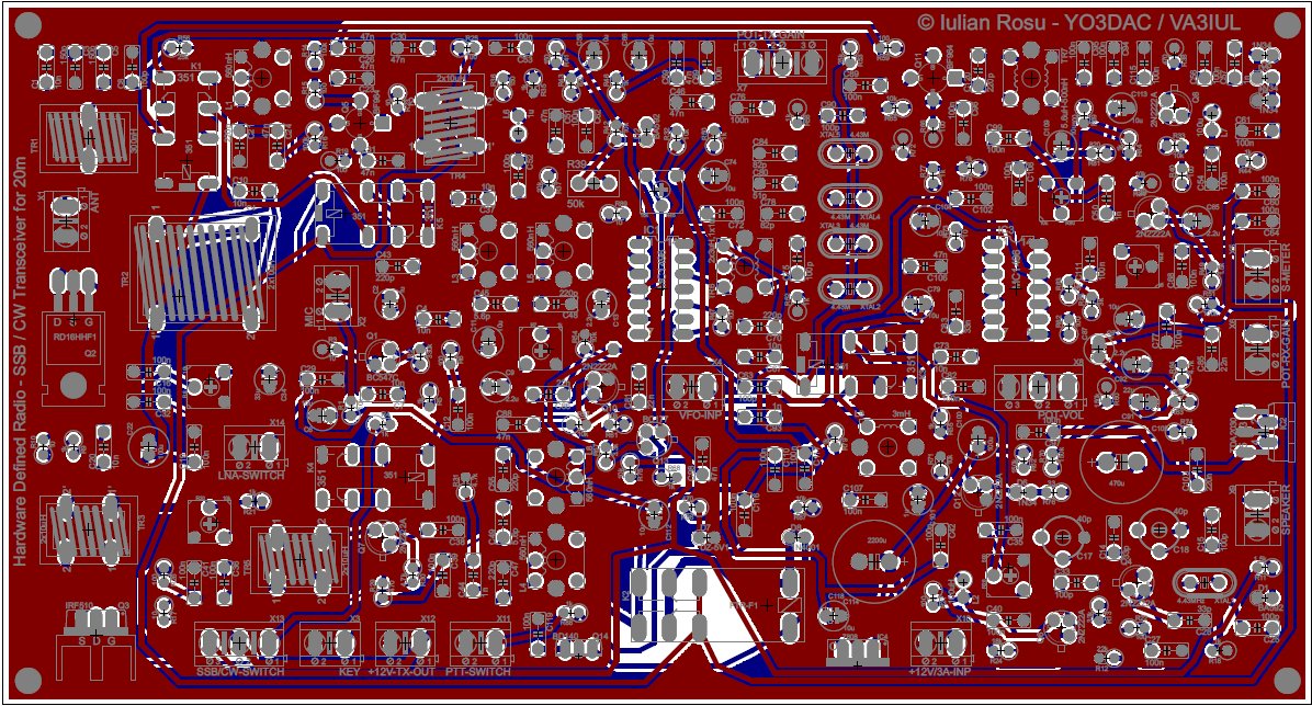
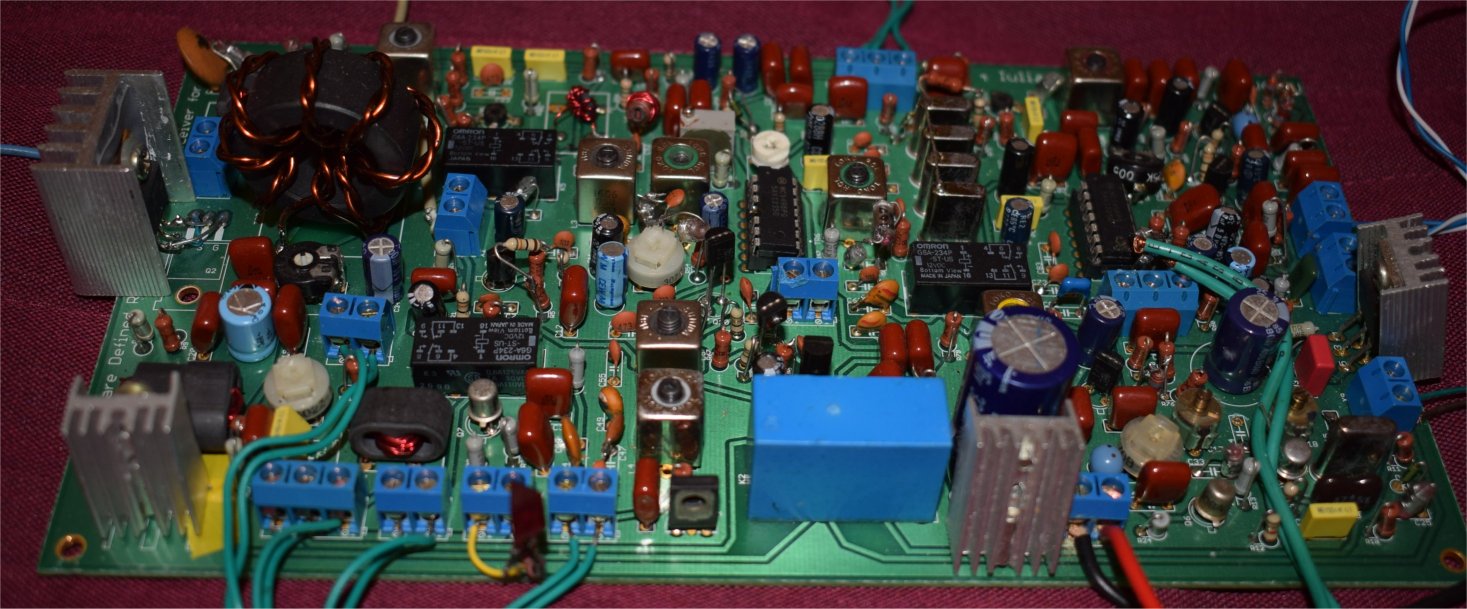
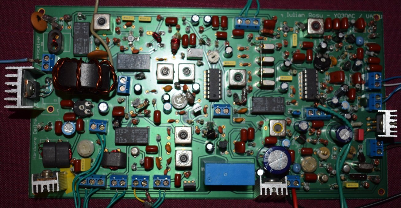
Take a look to the PCB layout and to the final circuit Picture1, Picture2
Here you can find pictures and contact recording of a version of the transceiver built by Adrian Navia, XQ6DWO.
Schematic Diagram
Block Diagram
Vackar VFO - 18.433 MHz to 18.783 MHz
Transformer Info
TR1 - Bifilar 2x10uH Ferrite Toroid
TR2 - Primary - Bifilar 2x3uH, Secondary - 1uH, IF Ferrite Can
TR3 - Primary 5.6uH, Secondary 500nH, IF Ferrite Can
TR4 - 2x10uH Ferrite Toroid
TR5 - 2x10uH Ferrite Toroid
TR6 - 2x10uH Ferrite Toroid
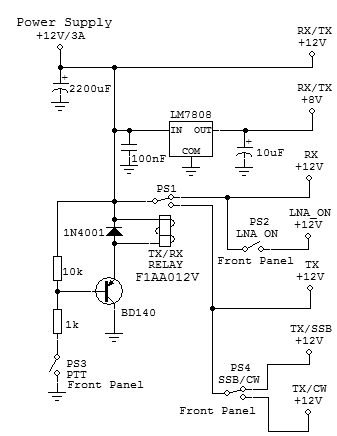
Power Supply Circuit