
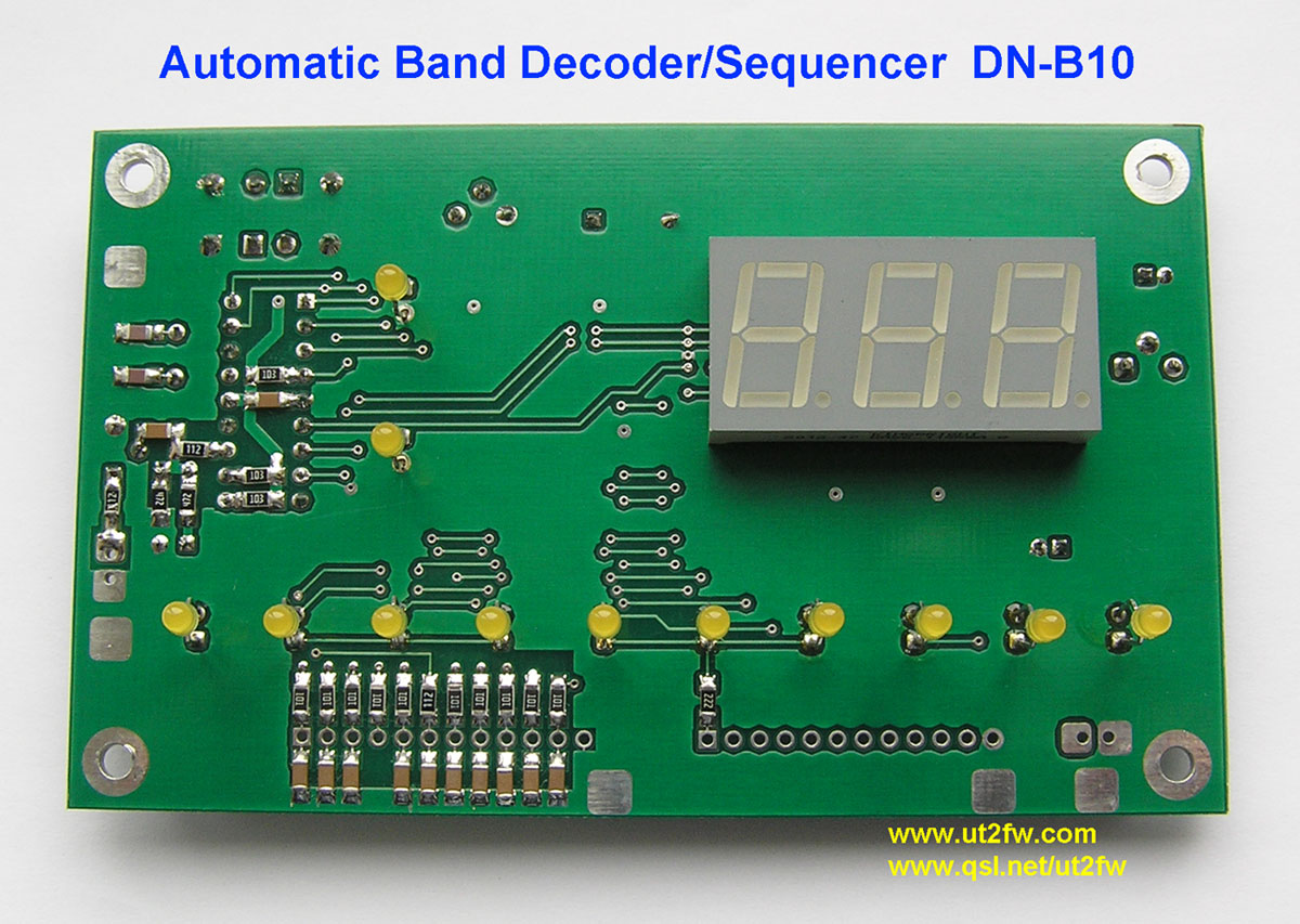
Automatic Band Decoder/Sequencer DN-B10
The main target to build the high-power amplifier is ensuring high reliability. If the protection of the amplifier had not carefully designed, an accident can happen at any inopportune moment.
All switching amplifier should be related to each other and operate by a single algorithm.
The functions execution algorithm required to consider both the characteristics of building amplifier, and the specifics of HAM Radio applications.
An important requirement for HAM engineering - low cost.
Band Decoder/Sequencer DN-B10 is based on these requirements.
The device is designed for automatic switching RX-TX, LPF filters, ATT and amplifier protection.
Can be used to automatically select or switch any devices in accordance with the frequency of the signal applied to the Band Decoder. For example, to switch antennas, filters, amplifiers.
The principle of operation of the Band Decoder based on measuring the frequency of the signal from the transmitter. (Automatic band change based on TX frequency.)
For stable operation of a sufficiently HF voltage from ~5V. Which corresponds to the power of 0.5 W with impedance 50Ohm.
The control of the Band Decoder based on PIC16F648A. The microprocessor frequency counter, determines the frequency of the input signal and sets the appropriate range. The minimum tuning step of frequency is 10kHz. Min and Max frequency for each band as follows:
1.0 - 2.5MHz – 160m;
2.51 - 4.0MHz – 80m;
4.01 - 8.0MHz – 40m;
8.01 - 11.0MHz – 30m;
11.01 - 16.0MHz – 20m;
16.01 - 20.0MHz – 17m;
20.01 - 23.0MHz – 15m;
23.01 - 26.0MHz – 12m;
26.01 - 31.0MHz – 10m;
31.01 - 55MHz – 6m;
The Sequencer controls the amplifier RX-TX switching. For safe switching, used certain sequence for switching. The algorithm burned to microprocessor.
The switching order for amplifier from RX-mode to TX-mode is as follows:
1. Band Decoder select the corresponding range LPF in the amplifier.
Next, the Sequencer is enabled from the PTT-signal from the transceiver.
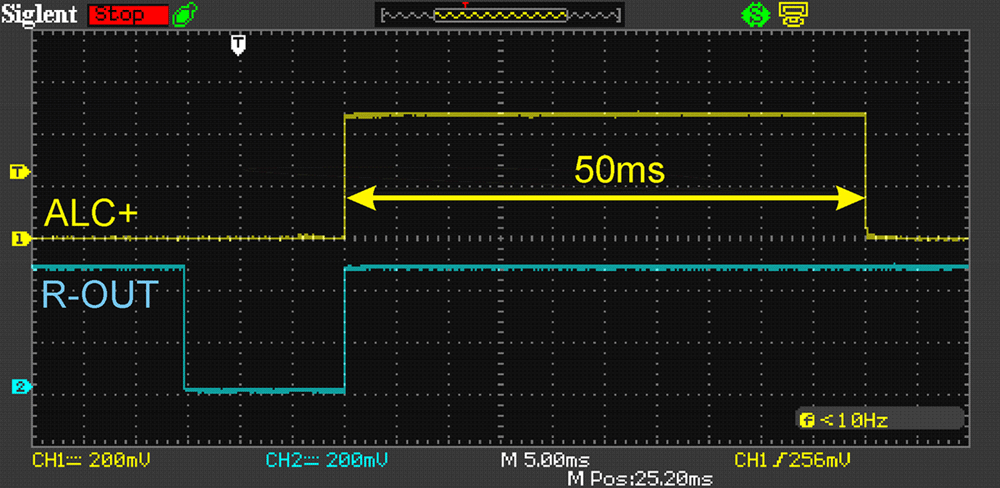
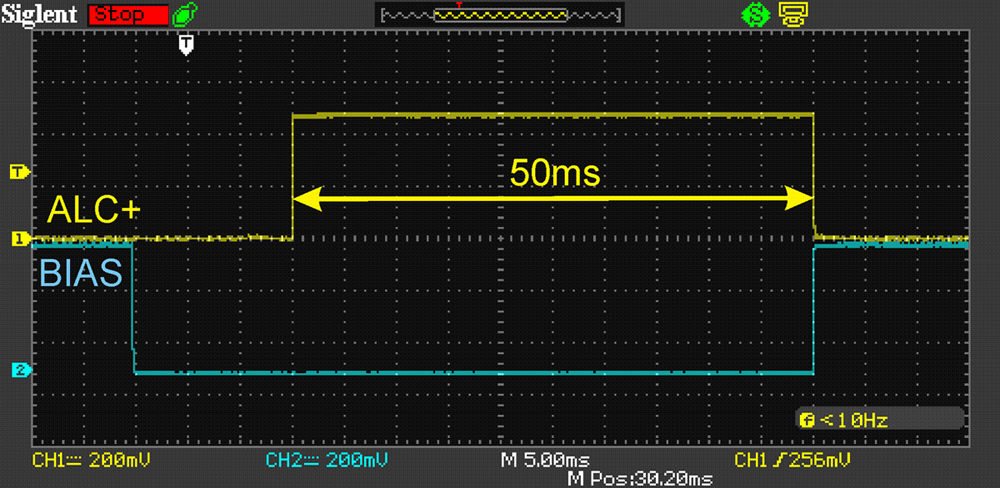
2. ALC reduces the power of the transceiver to 0W at 50mS.
3. Connect the ANT to amplifier. Relay delay is 40mS.
4. Connect the INPUT to amplifier. Relay delay is 10mS.
5. BIAS voltage.
6. ALC increases the power of the transceiver to nominal.
7. When returning the transceiver to RX-mode, the amplifier will be switched into RX-mode.
Band Decoder can operate like a standalone unit. It is enough, just to connect the frequency source.
Screenshots waveforms:
R-IN <–> R-OUT
R-IN <-> BIAS

ALC+ <-> R-OUT
ALC+ <-> BIAS
Additional features of Band Decoder/Sequencer
To get the same amplifier output power, use the attenuator between transceiver and amplifier. Band Decoder/Sequencer can control two attenuators. On each band, can be selected one of four states for attenuators:
1. Turn off both ATT.
2. Turns on ATT No. 1.
3. Turns on ATT No. 2.
4. Turn on both ATT.
The attenuators states, are hard coded into microprocessor.
Attenuators selection by bands:
160m, 80m, 40m, 30m – ATT1 on, ATT2 off.
20m, 17m, 15m – ATT2 on, ATT1 off.
12m, 10m, 6m – ATT2, ATT1 off.
Comparator can be used to control the amplifier protection circuits. For example, amplifier input overload protection. Comparator reference voltage may vary depending on band. Comparator operation, DN-B10 forms PWM separately for each band.
With two buttons, "more-less", can be selected the desired voltage level and write into the microprocessor memory. Press and hold button until the voltage reaches the desired value. On the indicators can be seen the voltage level in the range 1-255. The actual voltage at pin PWM will be from 0V to 5V. The values will be saved when you turn off the Band Decoder/Sequencer.


Connectors pinout
X1 Pinout
PIN |
SIGNAL |
DESCRIPTION |
1 |
+12V |
Output +12V. Connected in parallel to contact +12V X4. |
2 |
160m |
Open collector 74LS145. Current up to 80mA, voltage up to 15V. |
3 |
80m |
Open collector 74LS145. Current up to 80mA, voltage up to 15V. |
4 |
40m |
Open collector 74LS145. Current up to 80mA, voltage up to 15V. |
5 |
30m |
Open collector 74LS145. Current up to 80mA, voltage up to 15V. |
6 |
20m |
Open collector 74LS145. Current up to 80mA, voltage up to 15V. |
7 |
17m |
Open collector 74LS145. Current up to 80mA, voltage up to 15V. |
8 |
15m |
Open collector 74LS145. Current up to 80mA, voltage up to 15V. |
9 |
12m |
Open collector 74LS145. Current up to 80mA, voltage up to 15V. |
10 |
10m |
Open collector 74LS145. Current up to 80mA, voltage up to 15V. |
11 |
6m |
Open collector 74LS145. Current up to 80mA, voltage up to 15V. |
12 |
GND |
Ground. |
X2 Pinout
PIN |
SIGNAL |
DESCRIPTION |
1 |
PWR |
Input. Disable LPF relay control. Apply +5V. |
2 |
READY |
Indicate, if present a HF signal at frequency counter input |
3 |
BIASP |
Control for MOSFET bias voltage. TTL output +5V up to 10mA. |
4 |
PTT |
PTT input. Shorted to ground for TX-mode. |
5 |
R-IN |
Control for IN-relay. TTL output +5V up to 10mA. |
6 |
PWM |
Protection circuit control, voltage from 0V to + 5V. Current up to 0,5mA. Rl > 10k. |
7 |
ALC-G |
Control for transceiver ALC. Open drain up to 10mA, U<14V. |
8 |
ATT1 |
Control for ATT1 relay. TTL output +5V up to 10mA. |
9 |
ATT2 |
Control for ATT2 relay. TTL output +5V up to 10mA. |
10 |
ALC+ |
Control for transceiver ALC. TTL output +5V up to 10mA. |
11 |
R-OUT |
Control for OUT-relay. TTL output +5V up to 10mA. |
12 |
GND |
Ground. |
X3 Pinout
PIN |
SIGNAL |
DESCRIPTION |
1 |
Fin |
Frequency counter input. The minimum level is ~5V. |
2 |
GND |
Ground. Power supply. Chassis ground. |
X4 Pinout
PIN |
SIGNAL |
DESCRIPTION |
1 |
+12V |
Power supply +12VDC to +14VDC. The current consumption 80mA. |
2 |
GND |
Ground. Power supply. Chassis ground. |

Application of the Band Decoder/Sequencer.
The Band Decoder/Sequencer power needs sufficiently stabilized voltage 5V, current up to 80mA. But for the unification of the supply voltage applied additional stabilizer DA1 7805. Therefore, the PS input voltage may not be stable and range from +12VDC to +14VDC. The higher the voltage than the stronger will be heated 7805. Increasing the voltage will increase the power that is dissipated on DA1. Power is supplied to connector X4.
Limit voltage for input frequency Fin ~5V to ~70V. The optimal value of the voltage Fin ~15V to ~30V. The sensitivity of the Fin input is adjustable with variable resistor R27. Fin sensitivity input sets on a stable working of the frequency counter on all bands. To adjust the sensitivity of the Fin should be start with smaller power values. To start the adjustment in position of the rolling contact R27 closer to the ground pin. Frequency source, connected to X3.
To control Low Pass Filters relay, used DD6 74LS145D. The current limits one key of this chip is up to 80mA, voltage up to 15V. Key - transistor with open collector. LPF relay must be with diode shunt for surge reverse current protection. The keys output of the chip on X1 connector.
The remaining control signals Band Decoder/Sequencer on X2 connector.
Pin #1. PWR input. When applying + 5V, turns off DD6 74LS145D. DD6 can be turned off, if the amplifier can provide an additional control for relay from the LPF switch or transceiver.
Pin #2. READY output - TTL +5V, up to 10mA. The signal on this output will turn on READY LED. When HS detected on Fin input of frequency counter, Pin #2 will be +5V.
Additional control READY from the PTT signal.
If HF provided and PTT turned on, READY turns off simultaneously with turning off the PTT. If the PTT is turned off, then READY turns off with the disappearance of the HF signal on Fin input.
The READY signal can be used to enable (disable) devices at the time of availability of frequency and PTT.
Pin #3. The BIASP Output - TTL +5V, up to 10mA. Controls bias voltage for MOSFET. The BIASP signal appears after 50mS from R-OUT signal and 10mS from the R-IN signal. Time delay, allow to switch the relays R-OUT and R-IN. Thereby eliminating the accident of amplifier.
Pin #4. The PTT input. Shorted to ground. Sequencer control. The first will appear signals R-OUT, ALC-G, ALC+. After 40mS will appears R-IN. Then, after 10mS will appears BIASP and turns off ALC-G; ALC+. When you turn off PTT, READY, R-OUT, R-IN, BIASP will turn off.
Pin #5. R-IN output - TTL +5V, up to 10mA. The R-IN signal is formed by turn on the PTT. Controls to the input relay in the amplifier. R-IN signal will appears after 40mS after R-OUT tuned on. The time delay allows to reliably switch the R-OUT relay.
Apply powerful R-OUT relay. So to turn it on, takes more time. The selected time is 40mS. This time enough to turn on the vast majority of used types of relay. For R-IN, use an any low power relay. To turn on thouse types of relays, enough 10mS.
Pin #6. PWM output. The voltage on this output can be programmed from 0V to +5V. Load resistance for PWM should be at least 10k.
To set the voltage level, needed to enter the menu. Before turning Band Decoder press and hold any button. Turn on Band Decoder. Indicators will show tun. Set the desired voltage level by buttons. To save values, simultaneously press both buttons. Indicators will show SAF. Now, when you select a band, PWM value will be restored from the memory.
The Appendix contains the schematic of possible application the voltage of PWM in the protection of the amplifier.
Pin #7. The ALC-G output. Open drain. The key opens during switching relays R-IN, R-OUT - 50mS. The ALC-G signal appears only when the PTT signal exist. The ALC-G function is designed to reduce power of transceiver to 0W. If you do not reduce the power of the transceiver during switching the relay in the amplifier, it may damage the amplifier. During relay switching, will not load for the transmitter of the transceiver. Accordingly SWR will rise sharply. Increased value of SWR can damage the exciter of the transceiver. Typically, low power TRX is not equipped with protection from high SWR. The absence of the load for this type of TRX, usually not damage its MOSFETs. But will burn the relay contacts R-IN, R-OUT of amplifier. That will lead to premature failure. And eventually damage of the amplifier.
The ALC system in various transceivers are arranged differently. The Appendix contains the schematic form the control voltage ALC.
Pin #8. ATT1 output - TTL +5V, up to 10mA.
Pin #9. ATT2 output - TTL +5V, up to 10mA.
The Appendix contains the schemes of use ATT1; ATT2.
Pin #10. ALC+ output - TTL +5V, up to 10mA. The function is similar to Pin #7 ALC-G. But a different type of control signal. The signal ALC-G appears only when the PTT signal. The Appendix contains the schemes of use ALC+
Pin #11. R-OUT output - TTL +5V, up to 10mA. The control of the relay of the antenna in the amplifier. Is formed when the presence of a signal PTT.
Pin #12. Earth GND. Connect the negative supply voltage.
The link to the YouTube page => https://www.youtube.com/user/UT2FW
Demonstration of work of Band Decoder.