2 m. Band VHF Antenna Pre-Ampilfier
 I have an old VHF transceiver a little-bit "deaf"! By adding the following VHF
pre-amp as 1st stage, the improving of sensitivity is spectacular. The pre-amp including also a
Band-Pass input filter which rejects any undesirable signal outside of 2 m. Band.
I have an old VHF transceiver a little-bit "deaf"! By adding the following VHF
pre-amp as 1st stage, the improving of sensitivity is spectacular. The pre-amp including also a
Band-Pass input filter which rejects any undesirable signal outside of 2 m. Band.
I had worked manytimes MIR Space Station (good old days!) and ISS nowadays, with this circuit as antenna
pre-amp and a simple 4 Elements HomeBrew VHF Yagi, always with excellent results.
I'm using also that as Antenna pre-amp for LEO Satellites (Mode-B), where the DownLink is into the VHF Band (145.9 - 146.00 MHz).
("click" here for MIR & ISS QSL cards)
There is nothing unusual on this VHF pre-amplifier design. I was just remindful with PCB of this circuit and the components which I have used (see SMD ).
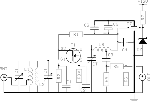
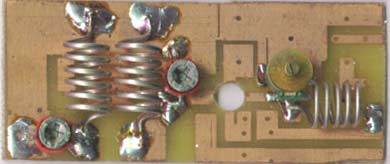
FIG. 1 shows the electronic circuit and FIG.2 the components layout.
FIG.1
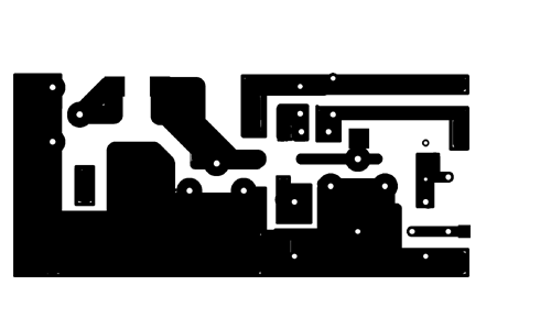
FIG.2
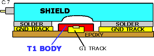
The "Green line" on FIG.2 it's a "shield" of tin-can material or small pieces of PCB between input-output . This piece of shield except the isolation it is necessary in order to be able to conduct the two opposite "Ground - tracks" on PCB ( GND A - main ground track and GND-B track).
You must be careful with shield and T1-Gate PCB track ! The shield (point "A" as shown in FIG.2) is a few millimeters above T1-Gate "PCB-track" without solder at this point
( see FIG.3 for details). It is possible to solder the pre-amp with the same tin-can material (or small pieces of PCB) on every side of PCB. This way we can make an RF-proof box by using as base the PCB of VHF pre-amplifier. The main PCB is "single-side" for simplicity, so the bottom shield (if used) is necessary to abstain at least 5mm from PCB's surface.
The PCB's arrangement looks like unusual with the opposite Ground-tracks and "link".
If you wondering why not a normal "continued GND-track" around components but this unusual design, the answer is simple: sometimes on VHF the PCB is very critical and usually it's the main source for various problems. Looking for a "single-side" PCB, which is easier contruction than a double-side PCB, I found after experiments that singularity with opposite GND-tracks connected by a "shield-plate" over T1 is "shot of" unwanted Ground-paths, offering an easy construction without problems and feedback during the operation. Repeating the construction many times, the result was always perfect, without problems. That is very important on a project, especially if that working on VHF area.
FIG.3
PCB: 29 x 64mm
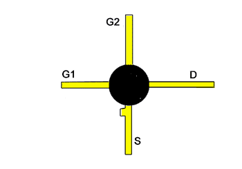
Top-view of BF981 |
FIG.4 shows the PCB and the BF981 view .
This type of VHF Pre-amp has a maximum gain of about 20 DB (depend on T1).
The Gain of my pre-amp is about 12-14 dB with input filter and output attenuator, but it's very "quiet" with excellent "Noise Figure", providing a very clean signal and that improving the weak signals. I think that its more important from a high amplification pre-amp.
The resistors R4-R5-R6 built-in a "PI" attenuation network in the circuit output ( Loss about 1 DB or greater - see table below). I have used this network for stabillity and good "50 Ohms" termination with the next stage, but on the other hand this network increasing a bit the noise level of the next stage, especially in case which the PI-attenuator is 3 dB or greater. Actually, if you are 100% sure about the stability of the next stage and you are looking for the maximum amplification with the best S/N, just remove the 3 resistors and take the output directly from C3 capacitor (not recommended). On the other hand, if you want greater attenuation (3 - 6 Db), the table below giving the values for R4, 5 & R6 in Ohms.
The Gain also depend on the coupling between L1-L2, but when these coils have bigger space between each other, the tuning curve is much-more sharpness.
 Keep in mind :
the BF981 Dual Gate MosFet is made for VHF antenna pre-amplifiers up to 200 MHz, offering excellent NF (Noise Figure), better than 1 dB (0.7 typical !!!) as describes the PHILIPS's DataSheet (see PDF below for details if you don't believe me !). In order to achieve this value, the current-flow through BF981 must be about 10mA. Thus, in order to adjust the circuit for the oprimum current, it is nessecary to remove the R3 and replaced it with a variable resistor (trimmer) 100 Ohms. Starting with maximum resistance on trimmer, with a mA-meter in series with +Vc (between R7-DZ Zener and C7), reduce smooth & slowly the trimmer's value till the optimum readout of 10 mA on meter-scale. After the adjustment, disconnect the Voltage supply & measure the value of trimmer. Then find a carbon resistor with equal resistance of preset-trimmer and solder this permanently (as R3). Before soldering cut the legs of resistor as short as possible (1mm).

"Click" here for BF981 Data Sheet (by PHILIPS Electronics)
Another important point is the Voltage between G2 & GND, must be 4 V for best NF in case which the +Vc is 10 Volts. On my circuit this quota is real, the R1-R2 divider gives the 40% of + Vc into G2, but that depend on the BF981 and your choise. However, you can modify the R1 & R2 divider for the otimum voltage feeding of G2 .
(* Of course all that, without input RF-signal on pre-amp !)
 For the best NF (Noise Figure) it's important the carefully tuning of CTs. Depend on the knowledge of constructor and the available Instruments on Shack, this VHF pre-amp gives a NF around to 1 DB. In addition, a small Hi-Q trimmer (optional) in series with Antenna, connected between central conductor of BNC-Input and TAP of L1, helps to achieve best "quietness" on receiving signal. Also is possible to vary the TAP on L1 between 1st and 2nd turn, till the best adjustment.
Of course, for Satellite use you must place the pre-amp as close as possible to your antenna (and not in the shack), with the necessary "change-over" relays. If you forgot it, the difference is: if the pre-amp is placed into the Shack and your Coaxial cable between transceiver and antenna has a Loss of about 3 DB, these "3DB"
is added in the NF of pre-amp and the NF now is 3 (coaxial) + 1 (pre-amp) = 4 DB !
So, down, into the Shack and "Noisy" or Up to antenna and "Clear"?
It's your choise..!
 Sometimes, on similar units is possible to occur unwanted effects widely known as "Feedback" or "paracitic oscillations".
This circuit, with this PCB did not have similar problems. However, the "parasitic oscillation" on a VHF pre-amp is possible to prevent as follow:
Sometimes, on similar units is possible to occur unwanted effects widely known as "Feedback" or "paracitic oscillations".
This circuit, with this PCB did not have similar problems. However, the "parasitic oscillation" on a VHF pre-amp is possible to prevent as follow:
1) put a 50-100 Ohms small resistor (0.25W) in series with G2. Both legs of resistor should be decoupled with GND by using 1nF SMD capacitors.
2) if the effect remains, then put a small ferrite bead (FB) through G2's leg, close to T1 body.
3) nothing yet? put a resistor 5 Ohms in series with Drain of T1, close to T1 body.
4) your last choise to prevent the "parasitic oscillation": put a ferrite bead through "Drain" leg of T1.
This method works 100%, but is unknown the action of FB on the circuit-response and in any case I don't agree with that. (When is absolutely necessary, try that).
5) Have you still "feedback"? The final solution: put your VHF pre-amp in.... garbage (Hi Hi)!
 Finally, I think this type of VHF pre-amp is excellent. The BF981 has low enough NF for VHF applications, without the necessity of use rare GasFet or HEMT components. Another advantage of BF981 is the low price and is commonly available on the majority of Electronic shops.
Since the environment's "noise level" on VHF band is high enough compared with UHF band, the NF-value of BF981 it covers 100% the requirements of Low-Orbit Satellites and it's unconditionally proposed as VHF antenna pre-amp.
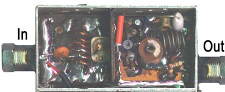
PCB of pre-amp with Coils and trimmers before the final construction
|
Another version of Pre-amp with simpler "input filter" (just one LC)
|

Old version of Pre-amp with RCA 40673 in place of BF981
|
Part List
T1 = BF981 (PHILIPS or TELEFUNKEN, avoid "No-NAME")
CT = trimmers 4-20 pF (Good Quality)
R1 = 82 K / 0.25 W (carbon)
R2 = 56 K / 0.25 W (carbon)
R3 = see text
R4, R6 & R5 = see Table below
R7 = 100 Ohm / 0.25 W (carbon)
C1 - C2 - C4 - C6 = 1nF SMD (or Trapezoidal-Ceramic)
C3 = 1nF / 63 V SM or ceramic
C5 = 10 uF / 16 V
C7 = 1nF (Feedthrough capacitor)
DZ = 10V / 1W Zener diode
L1 (air coil) = 6 turns, 1mm Silvered wire, length= 11 mm,
TAP. 1 1/2 turn from GND (cool-end), internal diam. = 6.3 mm
L2 = like L1 without TAP
L3 (air coil) = 5 turns, 1 mm Silvered wire, length 9 mm,
TAP. 1 1/4 turn from +VCC, internal diam.= 6.3 mm
"Pi" Attenuation Network Values
| ATT. |
R4 & R6 |
R5 |
| 1 DB => |
820 |
5,6 |
| 3 DB => |
270 |
18 |
| 6 DB => |
150 |
39 |
All resistors in OHMS / 0,25 W |
Good Luck de Makis SV1BSX (October 1995)
UPDATED: May 2004
| © COPYRIGHT: SV1BSX ® |
| Powered by |
 |