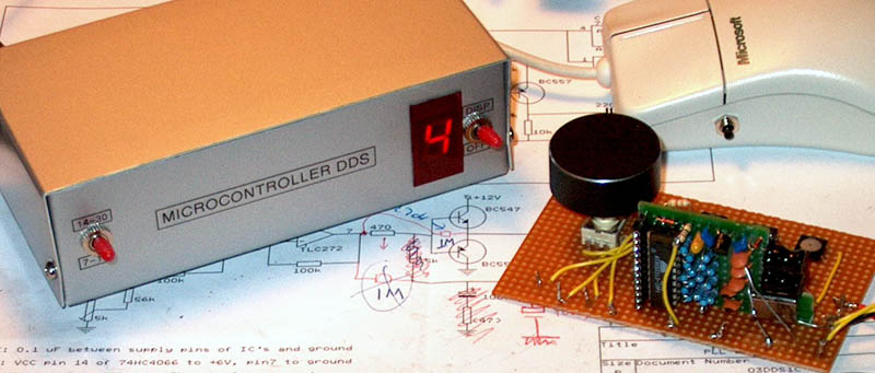
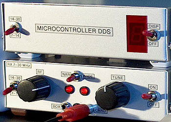
The Microcontroller DDS with PLL from 6 to 30 MHz and the
original DDS of Ton, PA0KLT with rotary encoder in a test setup.
EXPERIMENTAL DIRECT DIGITAL SYNTHESIS
BASED ON A MICROCONTROLLER AND
PHASE LOCKED LOOP
(2003 and modified in 2004)
NEDERLANDS ARTIKEL BENELUX QRP CLUB
The Microcontroller DDS with PLL from 6 to 30 MHz and the
original DDS of Ton, PA0KLT with rotary encoder in a test setup.
Frequency read out added to the microcontroller DDS circuit
In my version I added a simple one 7 segments display as a frequency display. So the usual combination of
a DDS chip plus a microcontroller to control the DDS and display the frequency is now reduced to just one microcontroller.
This single microcontroller works as a DDS, it displays the frequency on a 7 segments display and it scans the tuning
buttons.
Suppression of DDS spurious
A problem of using only 7 bits and the low clock frequency of 923 kHz is that there are some spurious signals.
However, they are efficiently suppressed in the PLL loop filter! If there are some left, they are weak and all within
the audio band. A big advantage is that they never cause any reception of unwanted signals as is the case with a
"normal" DDS without PLL. And they are completely gone when the RF frequency is tuned only 15 to 30 Hz up or down.
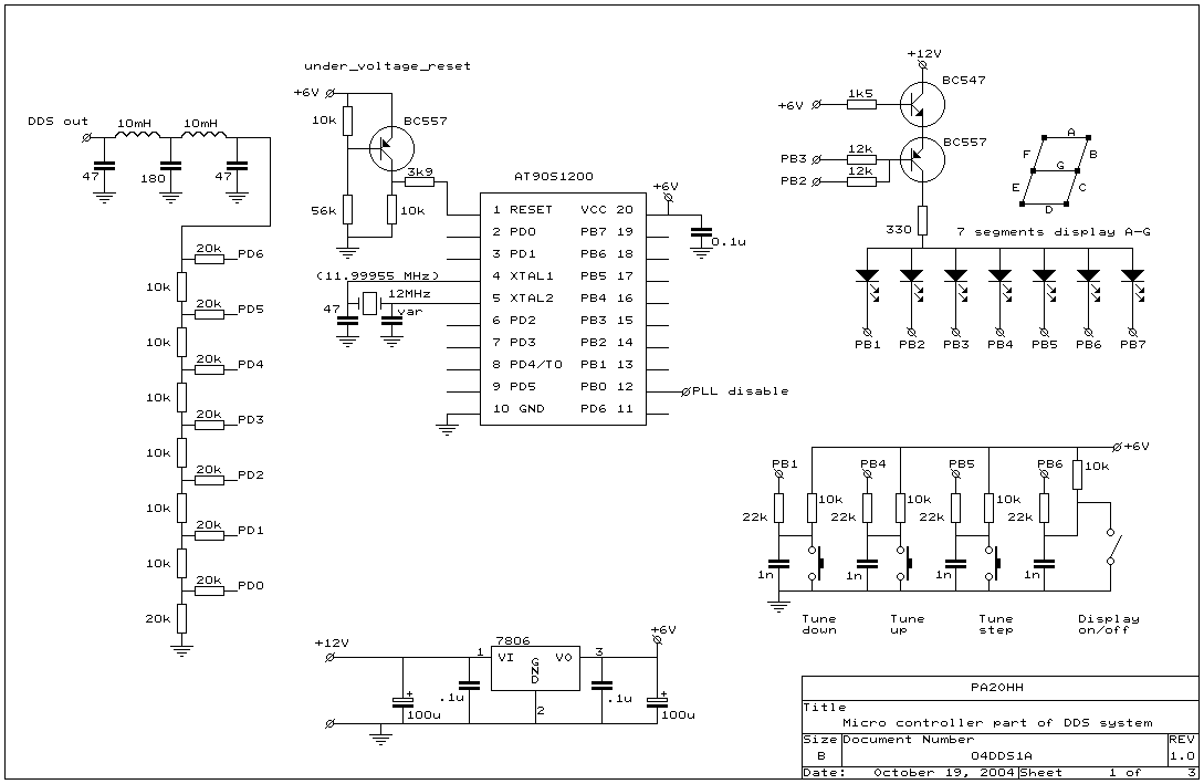
The Microcontroller DDS
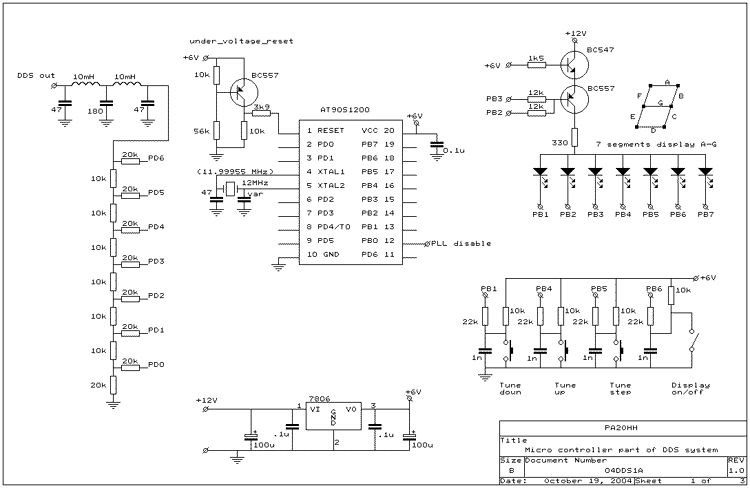
The DDS with microcontroller and display.
Output frequency 46875 Hz to 234375 Hz (RF frequency 6 to 30 MHz).
big diagram
The DDS Microcontroller
The heart of the DDS is the fast but simple and cheap microcontroller AT90S1200. The crystal frequency is
11999.55 MHz so a 12 MHz crystal can be used. The DDS controls a VCO with a frequency of 6 to 30 MHz.
The frequency of this VCO is divided by 128 and locked to the DDS with a phase locked loop circuit.
The frequency range of the DDS is then 46875 Hz to 234375 Hz.
One loop is 13 machine cycli so the clock frequency of the DDS is 11999.55 / 13 = 923.04 kHz. The output form
is not a sine but a triangle. The output port D, bits 0 to 6, is together with the resistor network,
the simple 7 bits D/A converter.
The L/C low pass filter has a cut off frequency of 200 kHz. Perhaps that an extra section might improve the performance
a little, as the cut off frequency is rather high compared to half the clock frequency of 923 kHz.
Ports B1, B4, B5, B6 are also used as inputs. In that case, the LED display is switched off by the BC557
transistor. The transistor is switched on by activation of one of the ports B2 or B3. The segments B and C of the 7 segments LED
are connected to these ports and one of the two is always on when a digit is displayed. Instead of a current limiting resistor
per segment, one resistor is used. You should expect that the
brightness varies a lot, depending on the number of segments activated. But in practice, it is hardly noticeable.
The LED is connected to the +12V to avoid variation of the stabilized 5V supply voltage due to the LED currents.
Disabling the PLL to avoid problems at high DDS output frequencies
Pin B0 disables the PLL during certain software routines when the clockspeed goes down to 1/8x 923 kHz. With such
a low clock speed that is even much lower than the highest DDS output frequency of 1/4x the clock speed,
the DDS output is heavily distorted for a moment. Without disabling the PLL (only 255 us) during these routines,
you can hear that as a loud click or "tjoop".
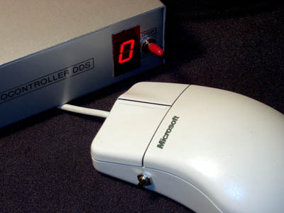
Tuning is done with 3 switches, two for tuning, one for the tuning speed.
I took an old mouse for it, only the 3 switches are used.
An extra switch is added as it was a two-button mouse.
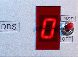
How can you read the frequency with only one display?
Very simple if you know it!
Frequency display
For the 3 lower tuning speeds, the kHz value of the frequency is displayed.
When the 10 kHz or 100 kHz tuning speed is selected, the MHz + 100 kHz value of the frequency is displayed.
That works as follows:
For a frequency of 21.345 MHz and 10 kHz - 100 kHz tuning speed:
Display "2" during 0.5 second
Display off during 0.1 second
Display "1" during 0.3 second
Display off during 0.1 second
Display "3" during 0.3 second
Then the display is off during 5 seconds and the frequency is displayed again.
For a frequency of 21.345 MHz and one of the lower tuning speeds selected:
Display "3" during 0.5 second
Display off during 0.1 second
Display "4" during 0.3 second
Display off during 0.1 second
Display "5" during 0.3 second
Then the display is off during 5 second and the frequency is displayed again.
The display is off during 5 seconds but the frequency is displayed immediately after the frequency up-down buttons are released.
The first digit is displayed a little longer than the others as this gives a more pleasant reading.
When the speed button is pressed, the speed (1 to 6) is displayed. It steps slowly (0.5 seconds per step) up or down when you also push one of the tuning buttons.
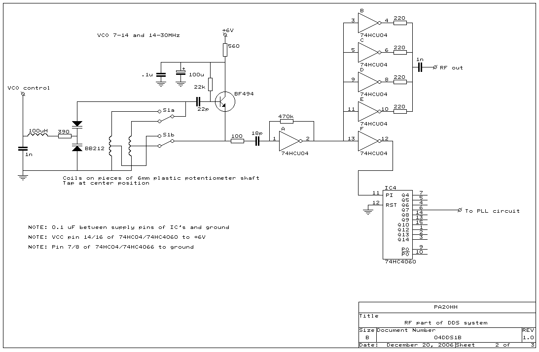
The VCO
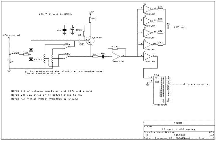
The VCO with output driver and /128 divider.
big diagram
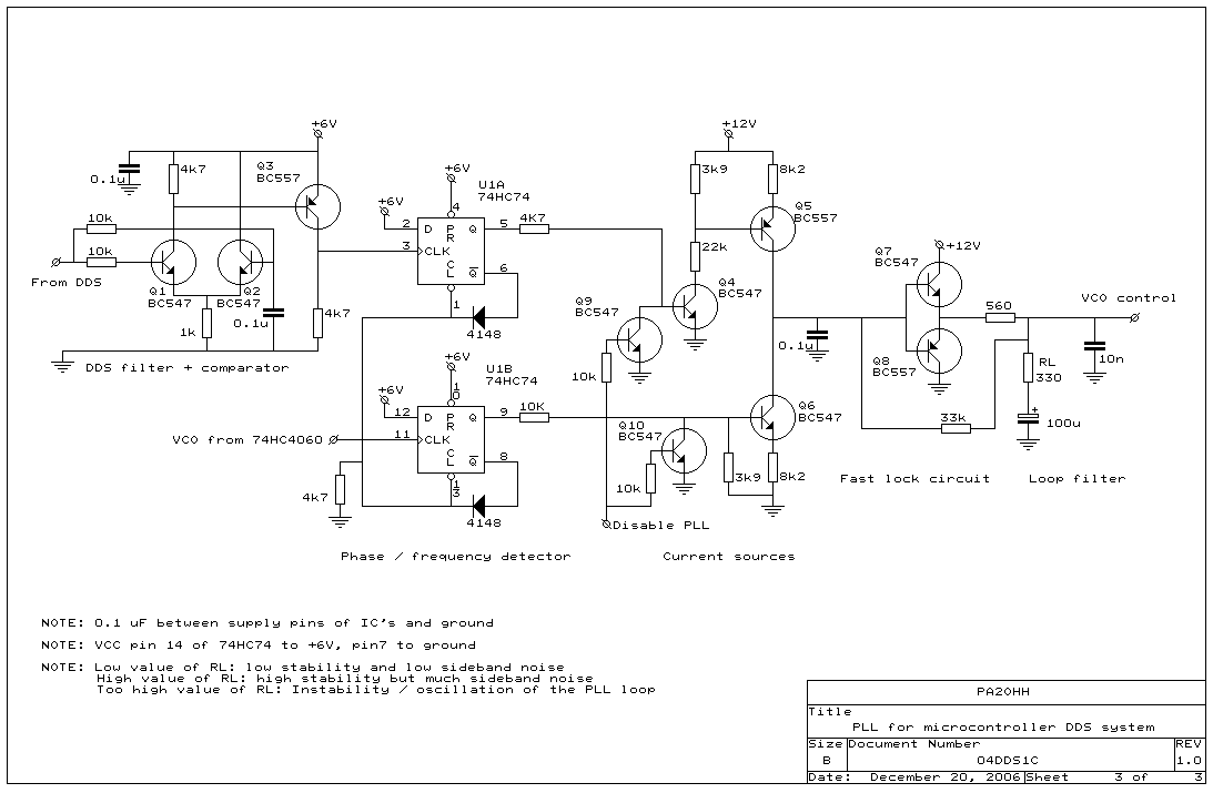
The PLL circuit
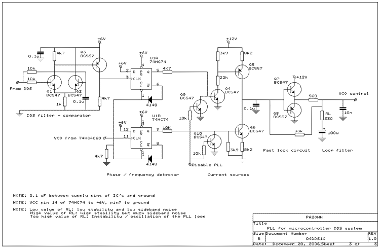
The phase locked loop circuit with the phase/frequency detector with charge pump.
Only standard, general available components are used.
big diagram
Standard components for the PLL
This is the usual circuit with a phase-frequency detector with set-reset flip flops.
The idea was to use a 74HCT9046 phase detector IC. But this part is not available anymore. That was for me the
reason to make such a phase/frequency detector with use of "standard" general available components.
Another advantage is that you have access to components and connections that normally are not accessible. It is for
example possible to disable the charge pump during certain software routines when the DDS output signal is distorted.
The PLL in detail
The 3 transistors Q1, Q2 and Q3 are a comparator circuit. The base of Q2 is connected to the average DC voltage of
the DDS circuit (averaged by the 10k resistor and the 0.1 uF capacitor).
The square wave output of the comparator circuit is connected to the clock input of the D-flipflop U1A. These inputs do have
a hysteresis circuit and do not need a perfect square wave signal. The VCO signal (divided by 128) is connected to
the second D-flipflop U1B. When both D-flipflop outputs are "1", they are resetted by the AND circuit consisting of
the two diodes 1N4148.
When locked, the D-flipflops with AND circuit do work as a phase detector, when unlocked, they work as a frequency detector.
The flipflop outputs do control the two current sources Q5 and Q6, who are charging the 0.1 uF charge pump capacitor.
The current sources together with the 0.1 uF capacitor do also effectively suppress all spurious signals.
The current is set by the values of the 8k2 ohm resistors. The voltage accross these resistors is 1V, the output control
voltage range of the VCO is from approximately 1.5 V to 10.5 V.
Finally you will find the PLL loop filter with the two transistors Q7 and Q8, who take care of a fast locking procedure
when the VCO is far off the working frequency.
Q9 and Q10 are the disabling circuit for the charge pump. The PLL is disabled during certain software routines when the DDS output is interrupted.

Interior of the DDS with PLL and VCO.
Software
Software for the AT90S1200
The trick is that changing the Frequency Tuning Word with a value of 36352 causes a frequency change of exactly 1 kHz
and that 36352 is 64x568. The smallest step used is therefore 568, giving 15.625 Hz frequency variation.
If the Frequency Tuning Word is changed, the decimal digits of the display are changed accordingly. There is one register
reserved for each decimal digit of the frequency. However, the lowest byte of that register is not a 0 to 9 counter but
a 0 to 64 counter. If the lowest byte exceeds 63 or is lower than 0, all other decimal values are adjusted.
This method was designed as all routines have to be an exact number of machine cycles, independent of what is happening.
If a button is pressed, the DDS clock is 1/8 of its normal clock speed of 923 kHz and the Frequency Tuning Word is
multiplied by 8.
However, it was very difficult to count all the machine cycles exactly so in the end I corrected the exact length of the
various routines by measuring the pulses of the charge pump with an oscilloscope, listening to the output signal with a
receiver and corrected various delays for best performance.
One NOP instruction too much or less is disastrous!
A frequency offset is programmed by setting (programming) initial values to the Frequency Tuning Word and the decimal digit registers.
Click this link to Download the Software for the AT90S1200: "04dds1soft.zip" with the
.ASM files needed to program the AT90S1200
Results
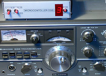
DDS used as 5 to 5.5 MHz VFO for an old TS520. Stability is good enough now for PSK31! |
DDS used as VFO for a simple Direct Conversion receiver that is connected to the soundcard of the PC. |
5 to 5.5 MHz VFO for a TS520
An extra switch is added later to switch a capacitor of 120 pF in parallel to the varicap of the VCO to make
it suitable for use as a 5 to 5.5 MHz VFO. I use it together with an old TS520SE, stability is better than the internal
VFO, good enough for PSK31.
VFO for a simple Direct Conversion receiver
The DDS PLL is used as VFO for a simple Direct Conversion receiver that is connected to the Soundcard of the PC.
Stability is perfect for decoding various digital signals with free available PC programs. Due to disabling
the PLL during the software routines when the clock speed is lowered, the PLL can work with high DDS output
frequencies without being disturbed.
There are almost no spurious signals within the audio band. If so, tune 30 Hz up or down and they are gone.
Using a microcontroller as a DDS is a very interesting idea, good for a lot of experiments in the future. I am sure than
you will hear more about it from Ton and other enthousiast amateurs.
The original DDS of Ton, PA0KLT
The original DDS of Ton, PA0KLT has a D/A converter with 8 bits and a sine output, the clock frequency is higher
and another PLL system is used. Tuning is done with a comfortable rotary encoder instead of 3 pushbuttons and he
has implemented features to set the minimum and maximum frequency, it has a frequency memory and
the tuning speeds are fully programmable. The microcontroller in his DDS is an AT90S2313 with more capabilities than
the AT90S1200 in my DDS.
Another advantage is that his DDS runs at half the clock speed during tuning and not at 1/8x during software routines.

RF signal without disabling the PLL during software routines when running 1/8 of the normal clock speed. |

And here with disabling the PLL for 255 us! |