ON7YD
ARDF timer

Select :
PartlistScematicsFunctional description
PCBDownloadDIP switch selections

Partlist
IC1 : PIC16C54XT *IC2 : 78L05Q1 : 3.2768MHzT1/2 : BC547c
C1/2 : 22pC3/4 : 100nC5/6 : 100pC7/8 : 100n
C9 : 10µF/10VR1 : 470R2/3 : 4k7R4/5 : 3k3
R6/7 : 1k8R8 : 8x47kS1 : DIP switch (8)D1/2 : LED 3mm

* : PIC16C54XT can be replaced by PIC16C84 or PIC16F84

back to top of this page
DIP switch selections (S1)

Switch 1-3 : identification
Sw 1Sw 2Sw 3Identification
offoffoffMOE (1st min. of 5 min. cycle)
onoffoffMOI (2nd min. of 5 min. cycle)
offonoffMOS (3rd min. of 5 min. cycle)
ononoffMOE (4rd min. of 5 min. cycle)
offoffonMOI (5th min. of 5 min. cycle)
onoffonMO (continue)
offononMOE (1st min. of 2 min. cycle)
onononMOI (2nd min. of 2 min. cycle)

Switch 4-8 : delay (value for each switch, add values)
Sw 4 : 30 min.Sw 5 : 1 hourSw 6 : 2 hours Sw 7 : 4 hoursSw 8 : 8 hours

back to top of this page

Functional description

This timer controls ARDF transmitters in accordance to the international ARDF rules. It can be used with 3.5MHz and 144MHz transmitters. Although it is small (PCB is 48x36mm), low cost and has a low power consumption (less than 5mA at 9 to 15V) it is a complete ARDF timer.

Identification (S1-1/3)
In addition to MOE- MO5 in a 5 minute cycle and MO (continious), a MOE and MOI in a 2 minute cycle are available (for training purposes).

Delay (S1-4/8)
A delay time up to 15.5 hours is programable. The delay starts after synchronisation and during this delay the timer will not drive the TX. This allows the organiser to hide the transmitters up to 15.5 hours prior to the first start, keeping the TX positions hidden for the competitors and saving the batteries.

RESET
After reset (pull RESET to ground) the timer will start with the active minute of the programmed TX, the delay-time is ignored. Switching the power on will have the same effect as reset. The processor reads the DIP-switches after reset (or power on), later changes of the switches will NOT AFFECT the programming !

SYNC
This input can de used to synchronise multiple timers. Pulling the SYNC input to ground for at least 1 second will 'alert' the synchronisation. The timers are synchronised when the ground connection is interrupted !
After synchronisation the SYNC input is disabled, so in order to permorm another synchronisation the timer has to be reset (or switched off).

TX
This output is pulled to ground when the TX should be active, otherwise it is 'open'. The voltages applied to the TX or KEY output should not exceed 30V, the current should not exceed 50mA.

KEY
This output is pulled to ground when the TX should be 'key-down' (3.5MHz) or modulated (144MHz), otherwise it is 'open'.

LED D1
Diode 1 has a double function. During synchronisation it will light as soon as SYNC is pulled low for at least 1 second (the timer is ready for synchronisation). During the 'delay time' D1 will light during the first second of the active minute, this allows a control of the synchonisation.

LED D2
When the TX is active D2 will light in the rythm of the modulation. If the voltage (from the TX) applied to KEY exceeds 15V a diode (eg.1N4148) in series with D2 is recommended.

+12V

The timer needs a supply voltage between 9 and 15V, the power consumption is less than 5mA (no LEDs lighting).

back to top of this page

Scematic diagram

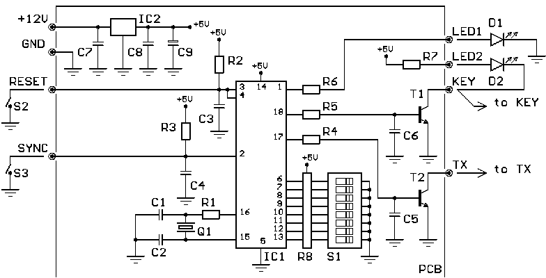
The scematic diagram is included in the download package.

back to top of this page
Printed Circuit Board

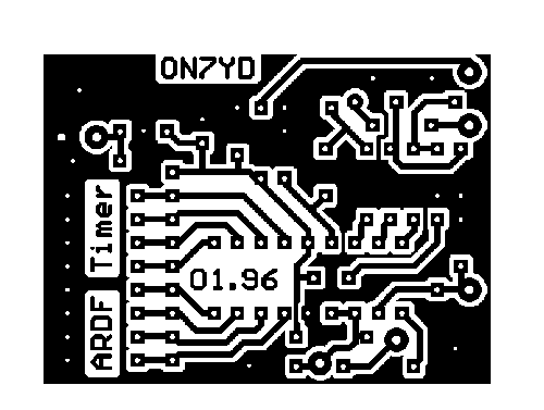
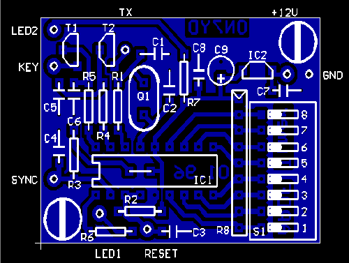
The exact dimensions of the PCB are 1.9 x 1.4 inch (48.3 x 35.6 mm).
A high resolution TIFF file of the PCB is included in the download package.

back to top of this page
Download

Click here to download a ZIP-file that contains :

back to top of this page

You are visitor number since 21 feb. 2000