144MHz ARDF
 transmitter
transmitter
transmitter
| Partlist | Circuit diagram |
| Functional description | |
| PCB | Download |
| IC1 : CD4093 | IC2 : 78L05 | IC3 : ICS501 | T1 : BC557c |
| T2 : BLU86 | T3 : BC557c | L1 : 2 x 8 wind. * | L2 : RFC ** |
| L3 : 8 wind. * | L4 : 8 wind. * | R1 : 220k *** | R2 : 180k |
| R3 : 100k | R4 : 1k | R5 : 220k | R6 : 47k |
| C1 : 10n *** | C2 : 10n | C3 : 1µ | C4 : 1n |
| C5 : 100n | C6 : 100n | C7 : 5-60p | C8 : 100n |
| C9 : 330p | C10 : 10n | C11 : 10n | C12 : 5-60p |
| C13 : 5-60p | C14 : 5-60p | C15 : 10µ/25V | C16 : 100n |
| * | : | L1, L3 and L4 = 0.2mm CuL wire on Amidon T20-12 |
| ** | : | L2 = broadband VHF choke |
| *** | : | for internal keying : R1 = 1M, C1 = 1µ/25V |
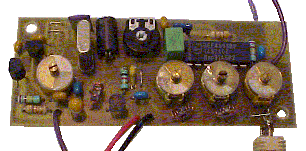
 Start the construction by cleaning the PCB and drilling all holes with 0.8mm (30mil). Enlarge the holes for R3,C7, C12, C13 and C14 to 1.2mm (50mil) and the mounting holes to 3.5mm (0.15 inch). Now check if all holes are drilled with the right diameter (this is your last chance to drill holes !). Next mount and solder the 2 SMD components (IC3 and T2) on the solder side of the PCB. Fixate the component with a small screwdriver (will also reduce the heating) and solder all pins. Avoid heating the components too much, if required ask a friend who has expercience with soldering SMD's. Be sure that IC1 in placed correctly (pin 1 is bottom/left). Now mount and solder all remaining components.
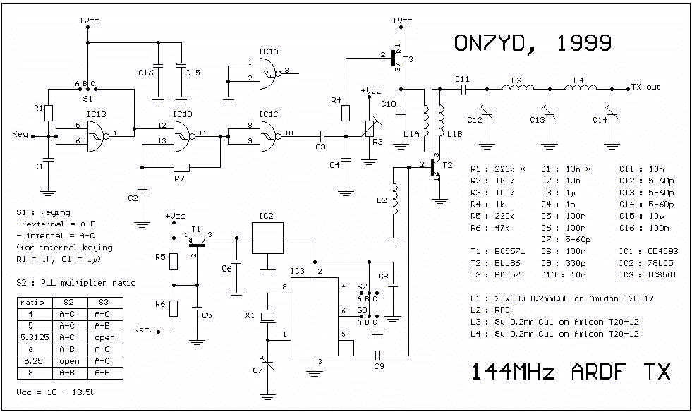 A high resolution TIFF file of the circuit diagram is included in the download package.
back to top of this page
A high resolution TIFF file of the circuit diagram is included in the download package.
back to top of this page

 The exact dimensions of the PCB are 3.075 x 1.30 inch (78 x 33 mm).