|
Wobbler & generator with PC controlled DDS Dr. Peter Halický, OM3CPH, Peter Halický, Jr., OM2PH Contents: Preface Description Construction Parallel port connector description and wiring Program Download Component list Professional solution by OK1UTS New!!! (July 2014) Roberto IW0RAQ pointed my attention to mistake in wobbler LPT pins assignment! Preface A few years ago, in 1998, we published the project of the universal DDS unit with Analog devices AD9850 (or 9851) chip. As an example of its use a simple program to control via PC was presented. After some time we created some more complex and hopefully more usefull application – PC controlled wobbler & sine wave broad band generator. The project now contains, except the universal DDS unit, detector, A/D converter with amplifier and broad band amplifier. The equipment is controlled by the originaly created program running at Microsoft Windows platform.
The device consists of the DDS unit based on well known Analog devices AD9850 or
AD9581 chip, simple broad band amplifier, diode parallel detector, TL081 (or similar)
based DC amplifier and Texas Instruments TLC549 8-bit A/D converter with serial data output.

Fig. 1: Block diagram of the device.
The DDS unit was used with very small modifications – filtering condensers at
4081 input were omitted to speed up the device and ENABLE input was wired
directly to +5V power source (as it is not used). 80 MHz clock oscillator
was used and output filter was set accordingly (AD9851 seems to be more
convenient, as it has built-in clock multiplication by 6 – low frequency clock
is easier to obtain, it can be found for example on failed PC mother boards).
The maximum frequency generated (at standard operation modus) is 1/2 of clock frequency.
DDS unit outputs sine wave with amplitude approximately 100 mV. It can
be sufficient for many applications. However, to get device more universal,
it was equipped with broad band amplifier with +20 dB gain and
-20 and -40 dB attenuators (Fig. 2). Who will need more attenuation can use more -20 dB
attenuators in series. 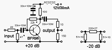 Fig. 2: Broad band amplifier and one segment of attenuator.
DDS unit, amplifier and attenuators have impedance close to 50 Ohm. The connection
to measured filter must usually contain appropriate transforming circuit. In the
case of LC based filters it is usually coil offset or capacitive transformer. The
situation is a bit more complicated in the case of crystal and monolithic filters
requiring usually complex impedance on both sides – usually R in parallel with C.
If this is the case it is possible to connect via resistive transformer (attenuator),
but with remarkable attenuation. 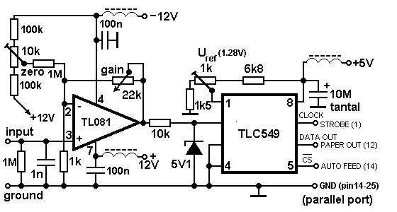 Fig. 3: A/D converter with amplifier.
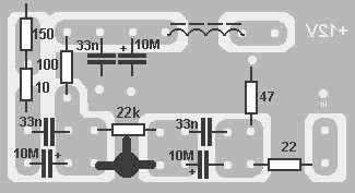
DDS unit was taken with no change (except of 3 condensers) as mentioned above. Broad band amplifier (PCB is on Fig. 4, components placement is on Fig. 5) was mounted directly onto switch on panel, the same way attenuators. The setup consists in collector DC current setup via change of the resistor between collector and the basis value and overall gain setup via setup of input attenuator (both resistors are marked with *). The amplifier is not shielded. 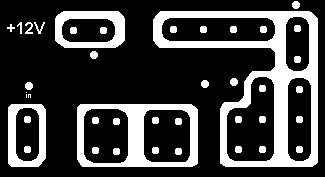 Fig. 4: Broad band amplifier PCB (1,5 x 2,75 cm).
Diode detector was placed into plastic tube (from marker) and connected with the device by shielded cable. As diode CB junction of AF139 was used. The emitter was broked and collector was soldered with housing. As input condenser it was used small tube-like ceramic one. A/D converter with amplifier (PCB is on Fig. 6, components placement is on Fig. 7) was not shielded. The whole device was powered from PC power sources. +5 and +12 V is available easily (red and yellow wire, respectively), -12 V must be taken from wire (usually blue), which must be identified on mother board connector. This must be done very carefully! Any soldering inside the computer should be avoided! All 3 power voltages were placed to a special connector at the back side of the PC close to parallel port connector. Those, who would like to avoid any change inside the PC, should construct some simple power source to feed the wobbler. 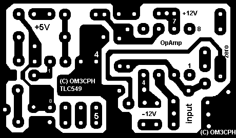 Fig. 6: PCB of A/D converter with amplifier (2,3 x 3,9 cm).
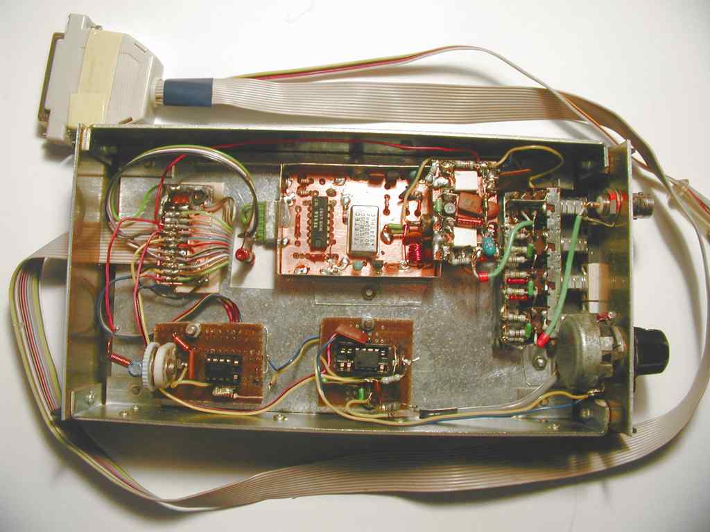 Fig. 8: The wobbler overall view (experimental design). Parallel port connector description and wiring.
Wires Data Bit 3, 4, 5 were disconnected from connector and used to conduct all 3 power voltages to wobbler.
The program to control DDS unit and to display results
of A/D measurements was
written for 32 bit Microsoft Windows platform. It was tested with Windows 98 SE,
Windows 2000 Professional. There are no special requirements for PC, except
it should have processor with 200 MHz clock or faster and it must have free parallel
port, of course. The faster the computer the faster the program is running.
With AMD/400 MHz and Windows 98 the maximum sweeping speed was 10 Hz. The same
computer, but with Windows 2000 gave only 3 Hz maximum sweeping frequency. Wobbler This is the main function. The window (Fig. 9a) is very simple and its use is very intuitive. 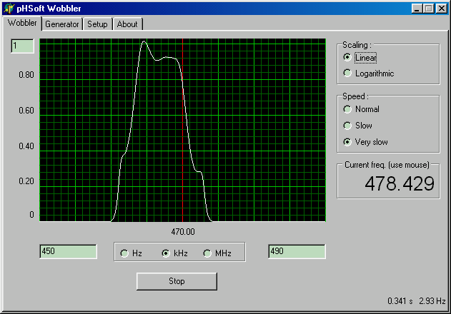 Fig. 9a: Wobbler window - linear display. The whole sweeping range of the generator is divided into 400 step frequencies of the DDS unit. This wobbler type doesn’t use continuous sweep. The step count is set constant. One can set only lower and upper limit (the first and the last step frequency). To make tuning easy it is possible to set multiplier – units, thousands and millions of Hz. At the vertical axis it is possible to display 256 distinct values (8-bit A/D converter is used). For convenience it is possible to set maximum value number (with no influence on A/D conversion, of course). The feature to use logarithmic display (Fig. 9b) is very useful. The maximum input voltage was used as maximum value for logarithmation. The approach is exact, but very convenient one. 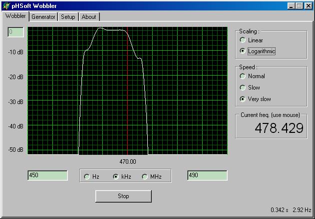 Fig. 9b: Wobbler window - logaritmic display. In the wobbler window there is possibility to set sweeping speed. It is a bit rough, but still convenient. For steep curves it allows to slow down sweeping to get more accurate curve view. The default value is fastest (“normal”). “Slow” and “Very slow” are achieved by repeated measurements at each distinct frequency and averaging. The side effect of slowing down is digital filtering of the data. It is important in the cases where input signal is very noisy. Generator This window (Fig. 10) gives basic DDS unit function – accurate frequency sine wave signal generation. Above and below the window there are buttons to tune up, and down respectively, in 1 Hz, 1 kHz and 1 MHz step. The buttons “+A” and “-A” serve for user defined tuning step. It's value is set in “A=” window. 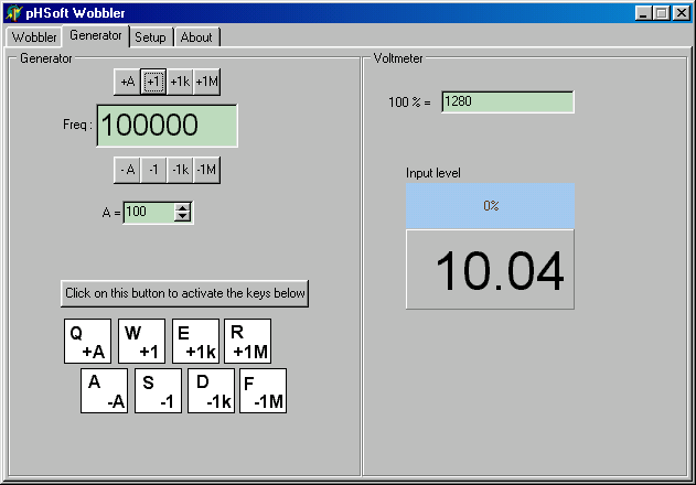 Fig. 10: Generator. Setup
Setup window (Fig. 11) allows to set address of parallel port which serves for
wobbler control. The value is set in hexadecimal notation, as usual. 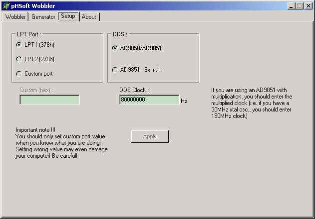 Fig. 11: Setup window. This window contains basic information about copyrights and Help button containing main part of this article. 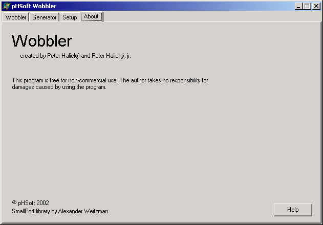 Fig. 12: About window. Wobbler control program can be downloaded and used for personal use free of charge provided copyright will be retained. Any commercial exploatation is possible only with agreement of authors. The authors don’t deliver or provide PCBs, nor the components used.
|