
By: Helge Granberg,
This unique push-pull/parallel circuit produces a power output of four devices without the added loss and cost of power splitters and combiners. Motorola MRF150 RF power FET makes it possible to parallel two or more devices at relatively high power levels. This technique is considered impractical for bipolar transistors due to their low input impedance. In a common-source amplifier configuration, a power FET has approximately five to ten times higher input impedance than a comparable bipolar transistor in a common emitter circuit. The output impedance in both cases is determined by the dc supply voltage and power level. The limit to the number of FETs that can be paralleled is dictated by physical, rather than electrical restrictions, where the mutual inductance between the drains is the most critical aspect, limiting the upper frequency range of operation. The magnitude of these losses is relative to the impedance levels involved, and becomes more serious at lower supply voltages and higher power levels. Since the minimum mounting distance of the transistors is limited by the package size, the only real improvement would be a multiple die package. For higher frequency circuits, these mutual inductances could be used as a part of the matching network, but it would seriously limit the bandwidth of the amplifier. This technique is popular with many VHF bipolar designs.
In paralleling power .FETs another important aspect must be considered: If the unity gain frequency (f� ) of the device is sufficiently high, an oscillator will be created, where the paralleling inductances together with the gate and drain capacitances will form resonant circuits. The feedback is obtained through the drain to gate capacitance (Crss), which will result in 360 � phase shift usually somewhere higher than the amplifier bandwidth. Thus, the oscillations may not be directly noticed in the amplifier output, but may have high amplitudes at the drains. This can be cured by isolating the paralleling inductance, which consists of the dc blocking capacitors (C7-C10, Figure 2) and their wiring inductance from the gates. Low value non-inductive resistors which do not appreciably affect the system gain can be used for this purpose.
FIGURE
1 - Photograph of the 600 Watt 2.0-30 MHz
MOSFET Linear Amplifier
CIRCUIT DESCRIPTION
Figure 2 shows a detailed schematic of the 600 W RF FET amplifier. It can be operated from supply voltages of 40 to 50 depending on linearity requirements. The bias for each device is independently adjustable, therefore no matching is required for the gate threshold voltages. Since the power gain of a MOSFET is largely dependent on the drain bias current, only gm matching is required, and it can be only � 10%.
FIGURE 2 - Detailed Schematic

The circuit board was designed to allow several different gate biasing configurations (Figure 3). In circuit "a", which is used in the amplifier described here, DI serves a purpose of preventing positive voltage from getting fed back to the bias source in case of a draingate short in a FET. This protects the other three devices from gate overvoltage. Cl-R2 combination establishes an RF shunt from the gate to ground, which is necessary for stabilization. R4 could also be used for this purpose, but it would have to be a relatively low value, resulting in unnecessary high current drain from the bias supply. Normally R4 is only a dc return to ground, which is required with DI preventing an open circuit in one direction. R3 is a low value resistor to prevent parasitic oscillations in a parallel FET circuit, as discussed earlier. Variations "b" and "c" are basically the same, except for R2, which can be used to control the amount of RF rectified by DI. In addition to blocking the dc in one direction, DI can be used for proportional biasing, in which the bias voltage increases with RF drive. This allows the initial idle current to be set to a lower than normal value, increasing the system efficiency.
FIGURE 3 - Various Bias Configurations

The gate de-Qing in these circuits is done with R4. Circuit "d" is another variation, where Dl is moved in series with R1 eliminating R4. The value of R1 must be high to prevent destruction from a drain-gate short. The common bias is derived from ICI (MC1723CP) which provides both line and load regulation. The line voltage regulation is defeated when the voltage to Pin 12 falls below 24 V, and the bias input can be used for Automatic Level Control (ALC) shut-down or linear ALC function. The regulator output voltage is adjustable from 0.5 to 9.0 volts with R5, which can be permanently set to 7.0-8.0 V. This voltage is also controlled by the combination of R10 and R25. R25 is a thermistor, and is tied to the heat sink for bias temperature compensation.
In Figure 2, the input from Tl is fed to the gates through C7-ClO and R15-R18. The input matching is initially done at the high end of the band (30 MHz). In contrast to a bipolar push-pull circuit, where the base-to-base impedance varies with class of operation, the gate-to-gate impedance of a common source FET circuit is always twice that from gate to ground. In this case, where two FETs are in parallel on each side, the gate-to-gate impedance equals the gate-to-ground impedance of one device. From the Smith chart information (Figure 4) this can be established as 3.45 ohms.
FIGURE 4 - Series Equivalent Impedance

The effect of R11-R14 and R21-R24 is minimal and can be disregarded. Considering the standard integers for Tl impedance ratio, 9:1 with its 5.55 ohms secondary appears to be the closest. This would set the values of R15-RI8 at 2.0 ohms each, which would result in 3.5 dB gain loss, and about 1.0 W would be dissipated in each resistor. For this reason it was decided to reduce their values to 1.0 ohm, and trim the values of Cl and C2 for lowest input VSWR. As a trade-off, the VSWR will peak slightly at 15-20 MHz, but still remain below 2:1.
Negative feedback is derived from a winding in T2 through R19 and R20. Its purpose is to equalize the load impedance for T1 and reduce the amplifier gain at low frequencies. Since the gate to source capacitance of a MOSFET is fairly constant with frequency, the amount of feedback voltage is inversely proportional to its reactance. This function should be more or less linear, unless the inductive reactance of Tl is too low, or if resonances occur somewhere in the circuit. No computer analysis (as in Reference 2) was performed on the negative feedback system. Instead a simple approach described in Reference 1 was taken, where the gain difference between 2.0 and 30 MHz determines the feedback voltage required to equalize the voltages of the secondary of T1 at these frequencies. With an input impedance of 45 ohms at 2.0 MHz, and the feedback source delivering 15 V(RMS), (Pout = 600 W) the values of R19 and R20 will be around 10 ohms each.
A ferrite toroid or a two hole balun type core can be used for T2. Relatively low ui material with high curie temperature is recommended, since the minimum inductance requirement for the dc feed winding is less than 2.0,uH. Depending on the material, T2 can reach temperatures of 200-250'C, which the wire insulation must also be able to withstand. Several different output transformer configurations (T3) were tried, including a transmission line type in Figure 5. Although difficult to make, it has the advantage that low ui, low loss ferrite can be used with multiple turn windings. At this power level, heat in the output transformer was a major problem. High permeability materials, required in the metal tube and ferrite sleeve transformers could not be used because of their higher losses and low curie temperature. On the other hand, low ui cores with larger cross sectional areas were not readily available. To reach the minimum inductance required for 2.0 MHz, two of these transformers, with low permeability ferrite cores were connected in series. Both have 9:1 impedance ratios. Alternatively the secondaries can be connected in parallel with twice the number of turns (6) in each. Cl 1 must withstand high RF currents, and must be soldered directly across the transformer primary connections. Regular mica or ceramic capacitors cannot be used, unless several smaller values are paralleled.
PERFORMANCE
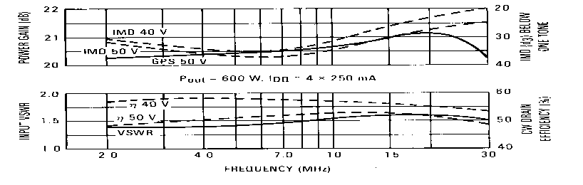
Due to the mechanical proximity of the four MOS FET devices, the RF ground of the circuit board is poor, and results in 1.0-1.5 dB gain loss at 30 MHz, which can be seen in Figure 6. The ground plane can be improved by connecting all source leads together with a metal strap over the transistor caps. Another method is to place solder lugs under each transistor mounting screw, and solder each one-to the nearest source lead. In this case, the heat sink will serve as the RF ground. Although the 3rd order IM distortion is not exceptionally good, (Figures 6, 7) the worst case 5th order products are better than -30 dB at all frequencies, and as can be expected with FETS, the 9th and higher order products are in the -50 to -60 dB level. It can also be noticed from Figure 6, that the IMD does not increase at reduced power levels, as common with bipolar amplifiers. The even order output harmonic content depends greatly on the device balance as in any push-pull circuit. The worst case is at the low frequencies, where numbers like -30 to -40 dB for the 2nd harmonic is typical. The highest 3rd harmonic amplitude of -12dB is at 6.0-8.0 MHz carrier frequency. Information on suitable harmonic filters is available in Reference 3. The stability of the amplifier has been tested into a 3:1 load mismatch at all phase angles. It was found to be completely stable, even at reduced supply voltages.
FIGURE 5 - Number of Turns Shown is not Actual

In a MOSFET (common source) the ratio of feedback capacitance to the input impedance is several times higher than that of a bipolar transistor (common emitter). As a result, a properly designed FET circuit should be inherently more stable, especially under varying load conditions.
It must be noted, that special attention must be given to the heat sink design for this unit. With the 200-300 watts of heat generated by the transistors in a small physical area, it must be conducted into a heat sink efficiently. This can be only done with high conductance material, such as copper. If aluminum heat sink is used, a copper heat spreader is recommended between the transistor flanges and the heat sink surface.
FIGURE 6

FIGURE 7
This bulletin is copied from Motorola RF DEVICE DATA BOOK Volume II by OH8JEP