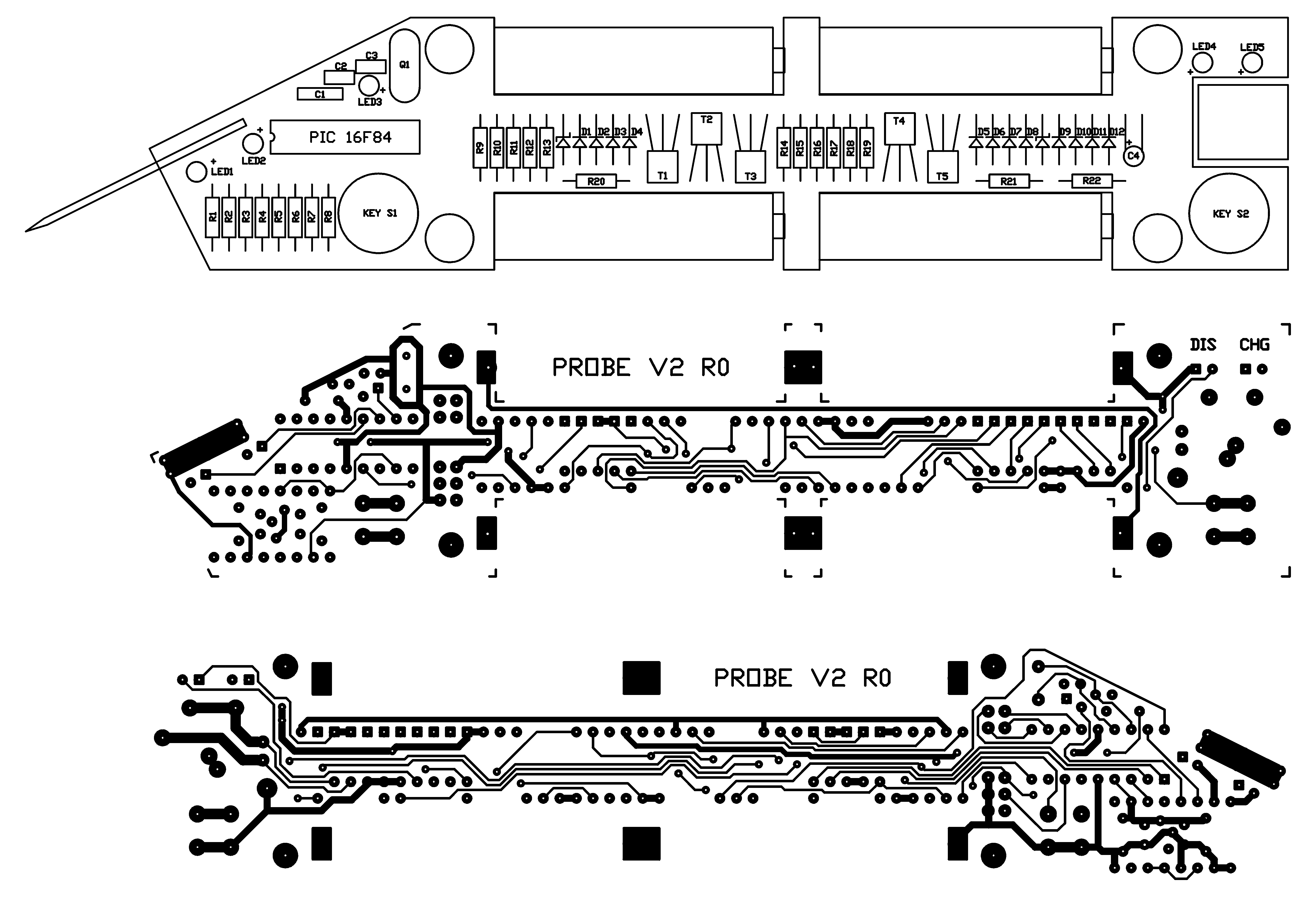
The Printed Circuit Board
The PCB is double-sided and approximately 39mm x 175mm before etching. In the end the board should be cut and pruned to exactly fit the same width as the LCD-module, 37mm (± 1mm or so). The length of the finished PCB is 173 mm at my prototypes. The cut for the battery-cells should also be matched to the exact length of the cells. This will make the construction more shock resistant as the cells are heavy and tin-solder is not very suited for mechanical loads.
When printing the transparent PCB layouts the scaling should be so that the distance between the LCD mounting-holes is 29mm x 108mm. I recommend to use the file probepcb.gif ("Save target as...") and print it to transparent films with a high quality laser printer.
Here are some other files:
| probepcb.zip | Contains the different PCB layers in .BMP- and .PDF-format files | ||
| probe1.pcb | PCB in Protel's DOS-format | ||
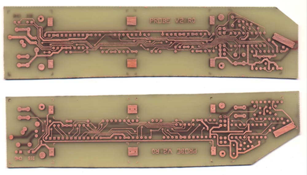
| Printed_Circuit_Boards.jpg | A picture of two etched PCBs. The upper one shows the solder-side and the other shows the component-side. |
Hint:
The trick to successfully (more or less) make a double-sided PCB is to first drill two 1mm holes in the board, at the mounting-holes for the LCD-module. The holes are drilled in two of the opposite corners of the LCD-module.
When placing the board at the transparent layout for UV-exposure you have to make sure that the two holes you drilled are matching the layout. Of course you do the same thing with the other side of the board. The more exactly the holes are drilled and matched to the layouts before UV-exposure, the better result!
Hint two:
Per Otto Vangsnes came up with a new idea of how to make the double-sided PCB. Here is what he did:
Get two thin (0,8mm) single-sided fibre glass PCBs and etch one of them with the component-side layer, and the other one with the solder-side layer. Drill some of the holes in each end of the PCBs. Make sure that you're beeing very precise and that you do the same holes on both PCBs.
Use sandpaper (grid 100) and sand down the fibre glass side of both PCBs till they have a rough surface. Then both of the surfaces are smeared wiht a very thin coating of two-component epoxy glue. The boards are then glued together, back-to-back. When doing this you should have wires or component pins through the holes you drilled. The wires must be as tick as possible to get an accurate fix of the two copper layers.
When the glue is hardened you can cut/file the exact shape of the board and drill the rest of the holes for the components. This method is easy and give a good result.
Good luck!
Erik Grindheim, 14.04.2000