Contact info:
Keith Bradshaw
P.O. Box 830688, EC
33
Richardson, TX 76080-0688
Phone: (972) 883-2099
Fax: (972)
744-9145
Current Capabilities:
The pictures of our capabilities are somewhat outdated, as of late we are building Microelectromechanical Systems (MEMS), and we have better than .25 micron (250 nanometer) resolution. We are working presently on comb drives using features of that resolution, which will greatly increase the work that the drive will be able to do proportional to drives 10 times its size. We are also doing micro-printing, making security labels the size of a speck of sand which have a name and serial number to track stolen goods.
My dream in the research is to drive a MEMS device using only RF energy, with no strings (wires or otherwise) attached. Imagine a remote control car 10 times smaller than a microscopic dust mite! That is my dream, and there are many others like it in our group. These are the tools we are using to realize these dreams....
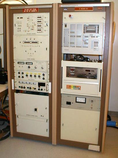
Pictures:E-Beam XIV, operational as of Feb. 20,
2000
SEM image of .5 micron lines, at 1 micron
spacing, shot 3/23/2000 on E-Beam XIV 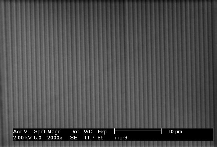
SEM image of the above lines, showing the
overlapping fields: 
Bay 3, where we do most of our lithography
work, the E-Beam is just on the other side of the glass door in the center of
the picture:
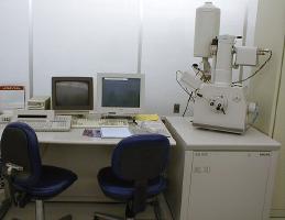
Bay 2, which houses the Scanning Electron
Microscope, the Atomic Force Microscope, and various optical
microscopes: 
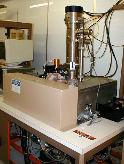
Our Phillips XL 30 SEM:

Justin
manning the SEM and using the EDAX to analyze the composition of a substrate.

Keith manning the
SEM, testing the capabilities of the E-Beam.
Our Park Scientific Atomic Force
Microscope: 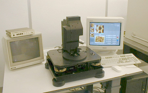
For more Pictures and a clickable map of all the cleanroom facilities, click here.
More to come!
Last updated: July 3, 2000