Cosy MUTO,
JH5ESM
11 April, 2009
Last modified: 17 May, 2009
![]()
A direct conversion receiver for 7MHz only made of single kind of general purpose PNP transistor is presented. No other semiconductor devices (even diodes!) are used. The circuit is built on a solderless breadboard so that it is easy to build, repair and modify it.
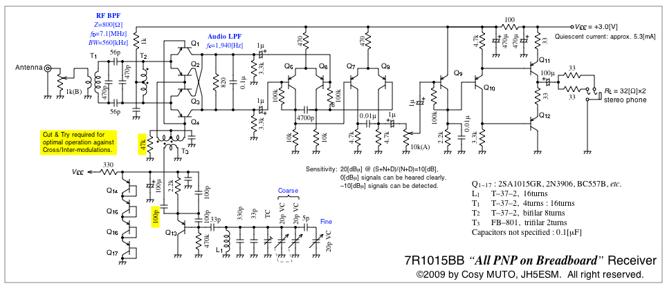
Fig.1 7R1015BB schematic (Click figure to enlarge, or click here
to download PDF version).
Figure 1 shows entire schematic of the receiver. As you can see, it is a simple DC receiver configuration.
Input RF signal is converted into differential (balanced) mode by T1 and then bandlimitted.
The
mixer (Q1~4) is doubly balanced type, however, device matching between
Q1 through Q4 and collector resistors (3.3[kΩ]) are not checked. In fact, I picked up 4 pieces of 2SA1015
from a baggage (qty.: 200) without any measurments.
The mixer load resistance is set to 820[Ω] so that the
primary-secondary winding ratio at T1 is given by 4.
By connecting 0.1[µF] capacitor in parallel to mixer load, it acts as a
first order LPF with 1.94[kHz] cut-off.
The mixer output is led to two stage differential amplifiers.
The
most significant drawback in DC receiver is AM feedthrough due to
mixer's second order distortion. Balanced mixer supress these
feedthrough in normal (differential) mode, but still remains in common mode.
That's why I adopt differential amplifires to reduce remained AM
feedthrough by their CMRR performance.
Audio
amplifier is a classic SEPP circuit with CE division driver. It drives
headphone or earphone. The total gain throughout receiver is approximately 70[dB] so that it
requires additional amplifier to drive loud speaker.
It is important
to make sure the phase compensation in high gain amplifiers. In this
receiver, it is performed by collector load capacitors in each stages
and supply line decoupling filter.
VFO is LC tuned type with
coarse and fine knobs to avoid to use expensive (and less opportunity to obtain) ball-drive unit or
vernier dial. It covers 6.940~7.270[MHz], where the fine knobs covers
approx. 15[kHz] range.
VFO supply is stabilized by four series connection of diode connected
transistors.
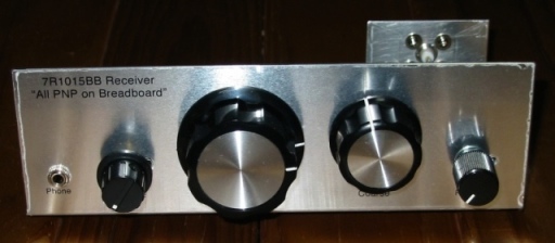
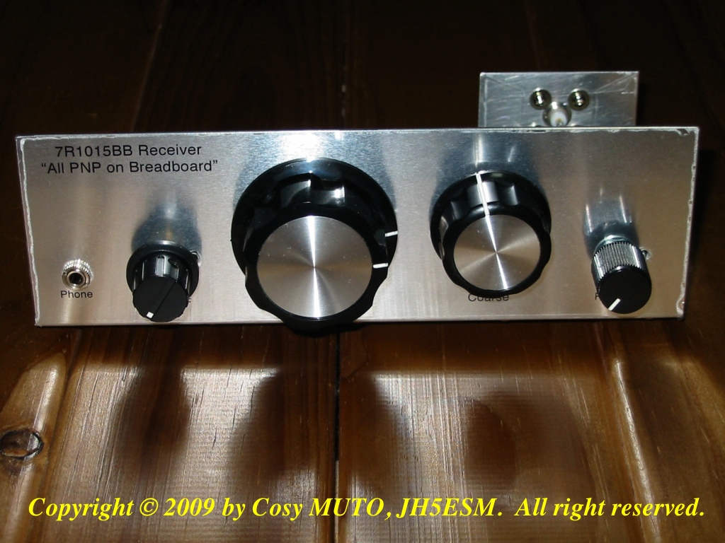
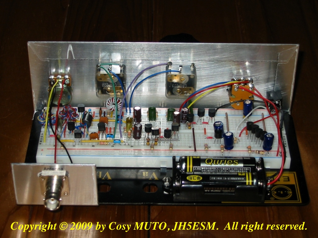
The reciever is build onto a solderless breadboard (e.g. WBU-202) as shown in Fig.2, where alminum front and rear panels are placed on it for operation.
Front panel layout is: headphone jack, audio volume/power switch knob, fine tuning knob, coarse tuning knob and RF ATT knob (left to right).
 |
 |
 |
| (a) Front view. | (b) Breadboard layout and routing. | (c) Rear view. |
| Frequnecy range | 6.940~7.270[MHz] |
| Sensitivity | 20[dBµ] @10[dB] (S+N+D)/(N+D) |
| 0[dBµ] signal can be heared clearly. Minimum audible RF signal level is –10[dBµ]. | |
| Power supply | 2 AA cells (DC 3[V]) |
| RF connector | BNC, 50[Ω] |
| Audio output | 3.5[mm] stereo, 16~32[Ω] |
| Supply current | 5.3[mA] |
| Dimensions | W183 × H60 × D98 [mm], excludes knobs, connectors and so on. |
| Mass | 0.32[kg] including batteries. |
![]()
![]()