K2 Elecraft and ... transverters
(automatic switching)
|
|
photo gallery
![]() Cliccare sulla foto per vedere la massima grandezza con
la miglior qualità
Cliccare sulla foto per vedere la massima grandezza con
la miglior qualità
![]() Click
on a picture to view it full size with full quality
Click
on a picture to view it full size with full quality
|
|
|
|
|
|
|
|
|
|
|
|
![]()
![]() La
mia costruzione è stata pubblicata su:
La
mia costruzione è stata pubblicata su:
![]()
![]() Radio Rivista -
giugno 2011
Radio Rivista -
giugno 2011
![]()
I transverters sono la mia passione, ne ho costruiti di
tutti i tipi: dai 50 Mhz ai 10 GHz.
Uno dei problemi a cui si va incontro è la scelta del tipo di apparecchiatura da
abbinare al transverter come IF. I transverters che coprono le gamme
radioamatoriali fino ai 432 MHz convertono la loro frequenza generalmente a 28
MHz, quelli invece a frequenze superiori usano l’IF a 144 MHz. Poi ci sono le
eccezioni come lo Javornik, di origine slovena, che converte a 14 MHz o alcuni
transverters per i 23 cm che convertono anche a 28 MHz.
Quando la conversione si ha a 28 MHz è molto comodo ed efficiente poter disporre
di un rtx che per natura sia già predisposto all’uso con transverters, e quindi
una commutazione che predisponga una bassa uscita in potenza (circa 100 mW) e
segnali rx/tx separati. Non sono molte purtroppo le apparecchiature HF che
dispongono di queste qualità. Io ho usato e sto usando ancora attualmente un
Kenwood TS850 … però avendo visto le caratteristiche dell’Elecraft K2 ho subito
pensato che con i miei transverters sarebbe stato il binomio perfetto.
![]()
Non è necessario che descriva le caratteristiche
dell’Elecraft K2, sono apparse in tutto il mondo recensioni su tutte le
principali riviste radioamatoriali e, poi, sul web c’è di tutto e di più.
Il K2 viene venduto dalla Elecraft in kit, il manuale (scaricabile dal web) è
fin troppo dettagliato e non occorre strumentazione per la taratura, poiché il
sistema di taratura è implementato nel firmware dell’apparato.
Il K2 è modulare e all’atto dell’acquisto bisogna decidere la configurazione
iniziale che vogliamo adottare.
In particolare c’è un modulo che ha attirato la mia attenzione: il K60XV (60 mt
/ transverter adapter). È un modulo che interfaccia il K2 con i transverters.
I segnali rx/tx sono separati e presenti su due connettori esterni. Il segnale
di IF è a basso livello (da 0.1 a 1.27 mW) e variabile dal comando Power sul
frontale. Si possono programmare fino a sei transverters che, se selezionati,
vengono inseriti in sequenza alle altre bande HF. Per ogni transverter si può
programmare:
- il valore di IF (7, 10, 14, 21 o 28 MHz)
- la visualizzazione della frequenza del transverter
- l’offset per correggere l’eventuale differenza di frequenza del transverter
(+/- 9.99 KHz)
- il limite massimo di segnale IF (normalmente 1 mW).
Queste caratteristiche hanno immediatamente attirato la mia fantasia in quanto
sarebbe stata un’ottima soluzione per pilotare i miei transverters per microonde
che si trovano remotati nel sottotetto.
![]()
I transverters per microonde (a parte qualche rara
eccezione) convertono i loro segnali a 144 MHz.
Mi serviva quindi un’altra conversione per poter utilizzare il K2 a 28 MHz.
Verso la fine del 2000 costruii l’ottimo
transverter per i 2 mt di I0FTG che mi
diede molte soddisfazioni e che pubblicai su RR agosto 2006, poi nel 2007 passai
alla costruzione di un altro transverter,
lo Javornik, che attualmente utilizzo
in banda 144 MHz.
Mi venne allora in mente di utilizzare il transverter di I0FTG per la
conversione dei segnali di IF dei miei transverters per microonde sul K2.
A questo punto mi serviva un ‘oggetto’ che mi commutasse automaticamente i
transverters semplicemente selezionando la banda interessata dal K2. Questo
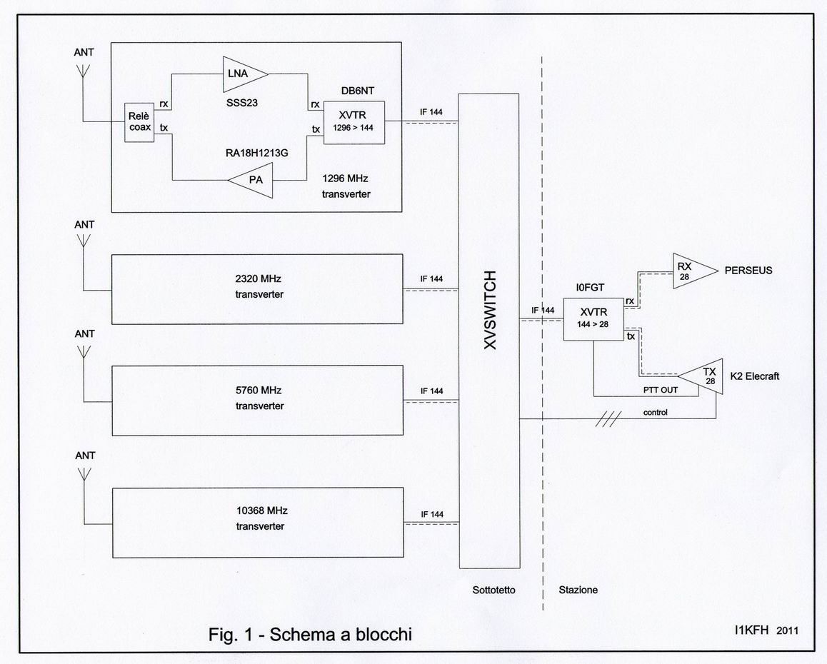
‘oggetto’ è composto da due schede: la XVOPTO e la XVSWITCH.
In Fig. 1 troviamo uno schema a blocchi che sintetizza il sistema da me
attualmente utilizzato: il K2 in trasmissione e il Perseus in ricezione
collegati ad un transverter per i 2 mt. e poi ai transverters tramite i due
moduli qui descritti.
![]()
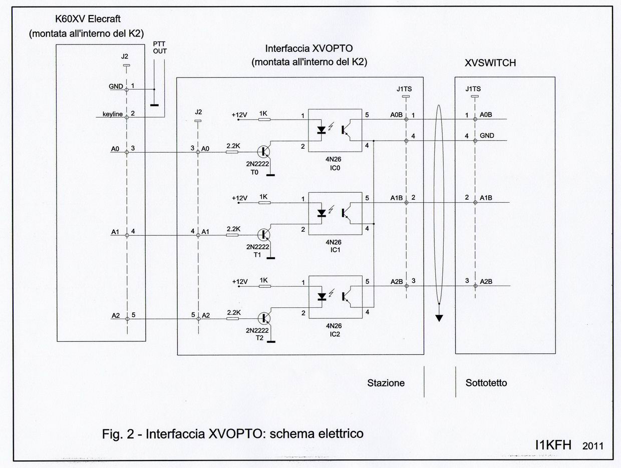
Il circuito e il suo funzionamento
Per capire il principio di funzionamento di questa mia interfaccia si deve
prima di tutto analizzare il funzionamento di una parte della scheda transverter
K60XV installata sul K2. Su questa scheda troviamo un connettore a 5 pin che si
chiama J2 e che è così configurato:
piedino 1 = GND
piedino 2 = XVTR KEYLINE (è il segnale di PTT del K2)
piedino 3 = XVTR SELECT 0
piedino 4 = XVTR SELECT 1
piedino 5 = XVTR SELECT 2
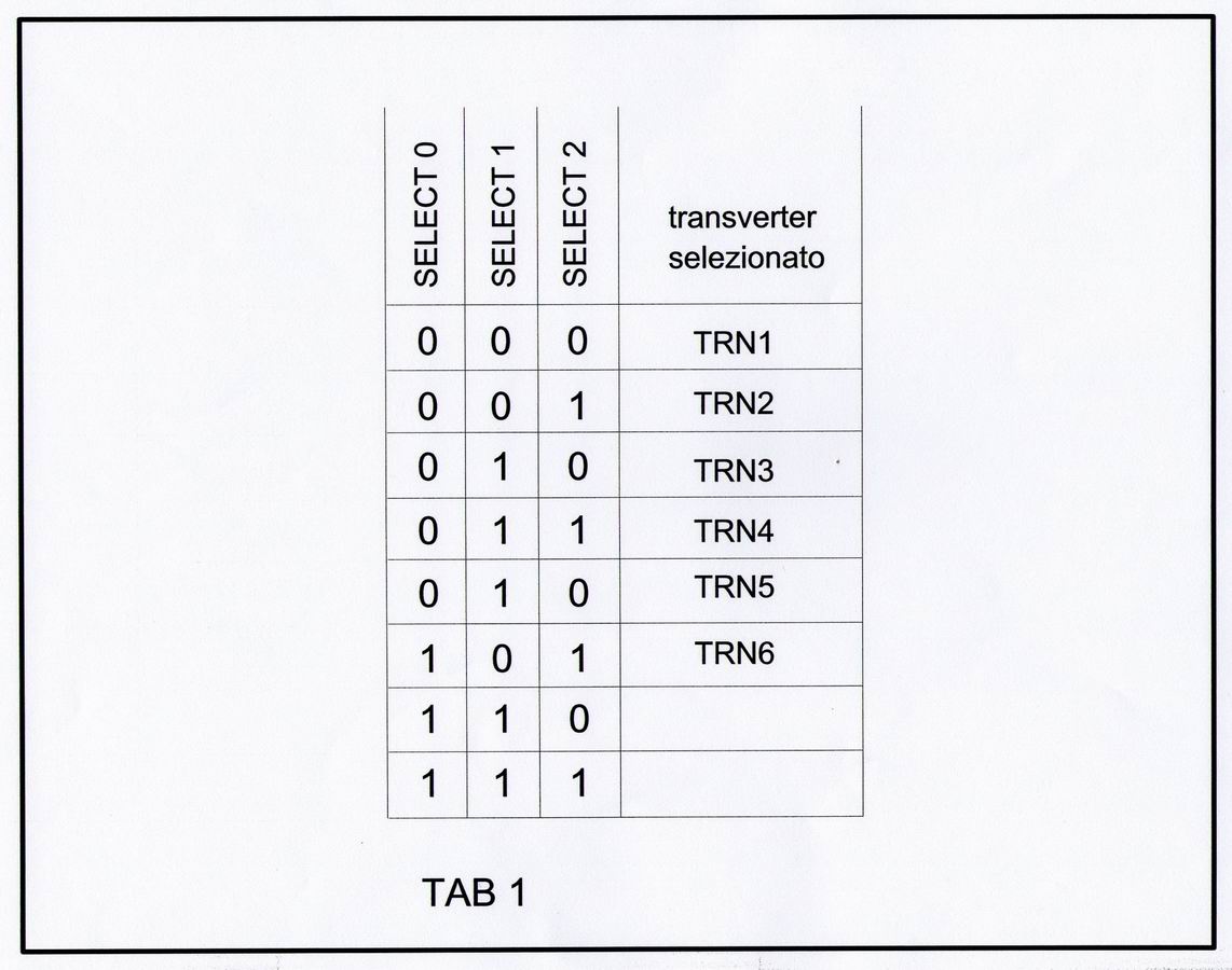
Esaminiamo i piedini SELECT 0, 1, 2 osservando la Tabella 1.
Notiamo che su
questi tre piedini troviamo un codice binario corrispondente alla scelta del
transverter in uso dal K2. Con soli tre fili (più la massa) riusciamo ad avere
otto combinazioni diverse, per cui usando un cavetto di quattro fili riusciamo a
trasferire a distanza l’informazione che ci indica su quale transverter stiamo
operando.
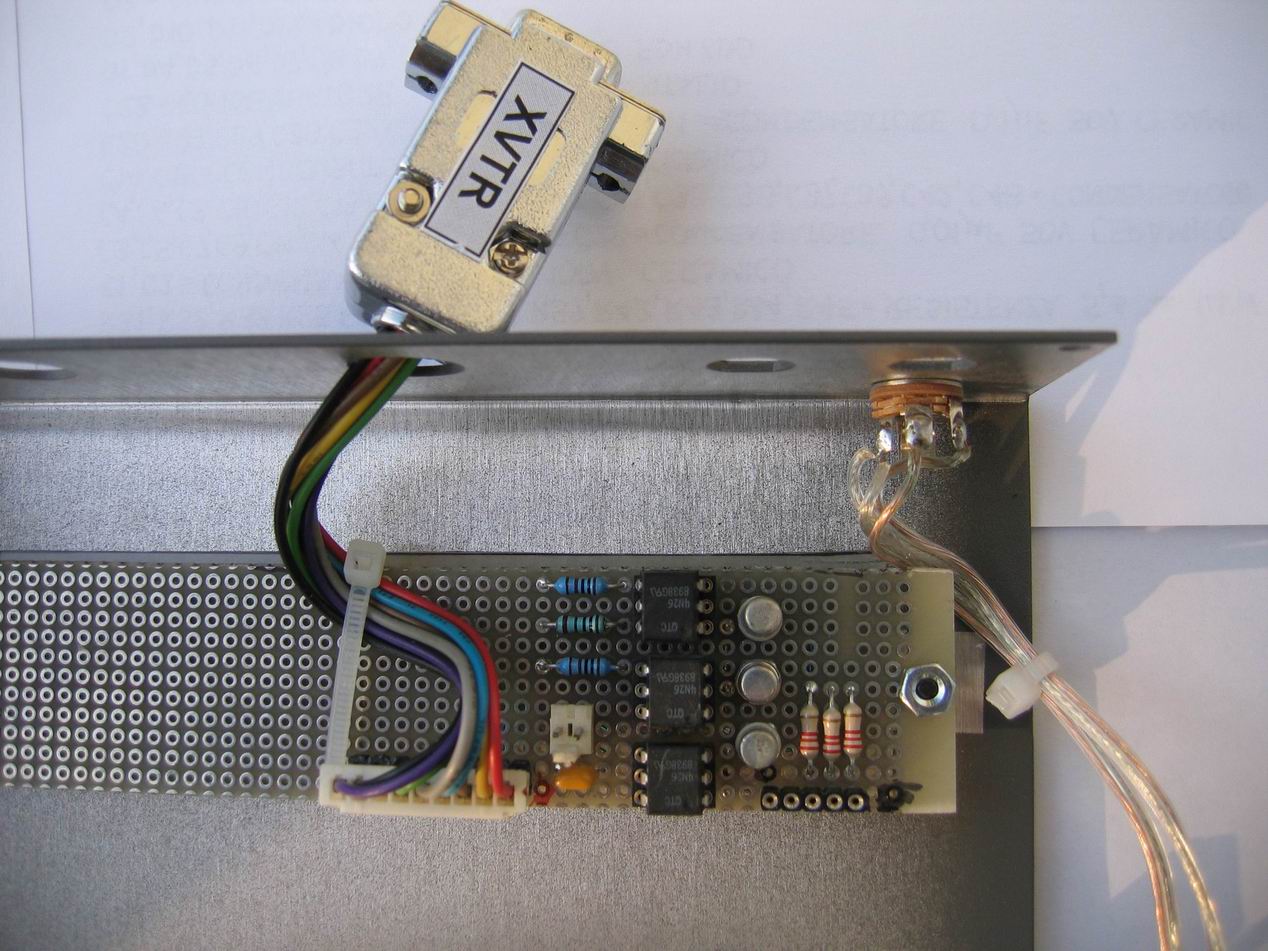
In Fig. 2 troviamo lo schema elettrico dell’interfaccia XVOPTO che non è niente
altro che la ripetizione opto isolata dei segnali SELECT 0, 1, 2. Usando
un’interfaccia isolata otticamente non vi è contatto fisico tra il K2 ed il
resto del mondo e si riescono a trasferire i segnali a distanza di decine e
decine di metri senza distorsioni. L’opto isolatore usato è il classico 4N26
pilotato da un transistor 2N2222. L’uscita del 4N26 è collegata direttamente ad
un cavo schermato per il trasferimento del segnale. I componenti
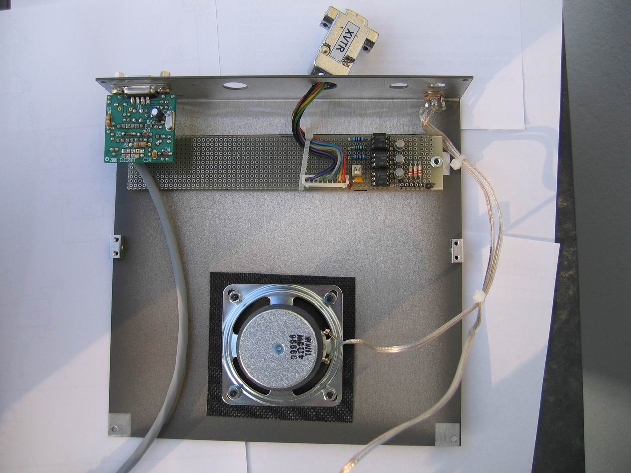
dell’interfaccia li ho sistemati su una piastrina mille fori fissata con due
viti nel coperchio superiore del K2, come si vede dalle foto. A montaggio
ultimato controllare bene il cablaggio, collegare l’alimentazione e i segnali
SELECT 0, 1, 2 dal K2 alla nostra interfaccia XVOPTO sugli appositi connettori.
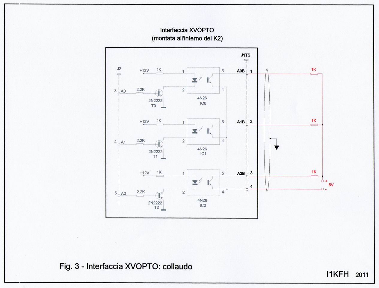
Il collaudo
A questo punto possiamo collaudare la scheda XVOPTO visionando il disegno
in Fig. 3 e precisamente la parte disegnata in rosso. Prendere un cavo di 4 fili
lungo una ventina di metri, o, meglio ancora, usare quello che poi collegheremo
al modulo XVSWITCH. Collegare un’estremità del cavo al connettore J1TS e l’altra
a tre resistenze da 1 Kohm e , infine, ad una sorgente di alimentazione di 5
Volt.
Impostare sul K2 il transverter n.1 (TRN1) facendo riferimento al manuale per
tutta la sua configurazione, poi con un tester controllare all’estremità del
cavo (dove ci sono le resistenze) che il piedino 1 di J1TS (A0B) si trovi a zero
Volt e i piedini 2-3 a circa 4 Volt.
Impostare successivamente sul K2 il transverter n.2 (TRN2) e leggere con il
tester zero Volt sul piedino 2 e circa 4 Volt sui piedini 1-3.
Impostare poi sul K2 il transverter n.3 (TRN3) e leggere con il tester zero Volt
sui piedini 1 e 2 e circa 4 Volt sul piedino 3.
Impostare infine sul K2 il transverter n.4 (TRN4) e leggere con il tester zero
Volt sul piedino 3 e circa 4 Volt sui piedini 1-2.
![]()
Il circuito e il suo funzionamento
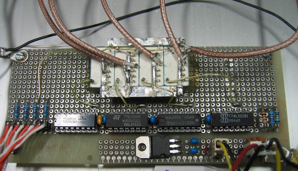
Lo scopo principale di questa scheda è quello di convertire i segnali dal K2
in forma binaria in segnali di natura decimale e poi, tramite relè coassiali,
comandare i nostri transverters remotati.
In Fig. 4 troviamo lo schema elettrico della scheda XVSWITCH. Il circuito
integrato usato per svolgere questa funzione è il 74LS138 (decoder/demultiplexer).
Per capire in maniera dettagliata il funzionamento di questo componente si deve
fare riferimento al suo datasheet.
In poche parole comunque fornendo ai piedini 1-2-3 (A0-A1-A2) del SN74LS138 un
codice binario (nel nostro caso il numero del transverter selezionato) avremo un
solo livello basso su una delle otto sue uscite (7-9-10-11-12-13-14-15). Questo
unico livello basso ci dirà quale è il transverter in uso e di conseguenza
sapremo quale transverter comandare. Il circuito integrato 74LS00 (4 porte NAND)
viene usato come invertitore, così pure il 74LS04 (HEX INVERTER). Il 9667 o 2003
non è nient’altro che un buffer per il pilotaggio dei relè che sono del tipo
coassiale RK1/UM1 per circuito stampato. Questi relè anni fa si trovavano a
manciate sui banchetti delle fiere ad un costo irrisorio.
Per come è stata concepita questa scheda dobbiamo fare attenzione a non trasmettere un segnale di
IF a 144 MHz se essa non è alimentata (off) perché non abbiamo nessun relè
eccitato e quindi il nostro TX a 144 MHz non vede il carico: per evitare questo
si sarebbe complicato notevolmente il circuito e non mi sembrava il caso.
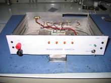
La costruzione
Questo modulo è stato assemblato su una basetta mille fori seguendo la
disposizione dei componenti di FIG. 5 e della
foto. I circuiti integrati sono
montati su zoccolo e i condensatori di by-pass da 100 nF devono essere
installati vicino all’alimentazione dell’ integrato stesso.
La basetta e i comandi trovano posto in un vecchio contenitore di alluminio
riciclato per l’occasione, come ampiamente documentato dalle foto. Sul pannello
frontale sono state inserite due boccole per l’alimentazione, l’interruttore con
led di accensione e 4 led per la segnalazione del transverter selezionato. Sul
pannello posteriore abbiamo un PL259 per l’IF principale che arriverà dal nostro
rtx per i 2 mt situato in stazione (nel mio caso il transverter di I0FTG),
quattro BNC che porteranno il segnale di IF ai vari transverter e infine un
connettore a vaschetta da 9 pin collegato al K2 in stazione.
Nulla di complicato quindi, si deve fare attenzione però al cablaggio dei relè
coassiali di commutazione dell’IF dei transverters. Il cablaggio relè-connettori
(BNC-PL) è da fare usando del cavetto in teflon flessibile da 50 ohm per
microonde, non per un questione di perdita di segnale, ma per poter saldare
tranquillamente senza fondere l’isolante. Le foto rendono l’idea di come fare per non rischiare
enormi perdite di segnali (siamo a 144 MHz).
Il collaudo
Questo modulo è meglio prima testarlo a banco simulando sul connettore J1TS
la combinazione per la selezione del transverter procedendo come segue:
TRN1 = collegare a massa il pin 1: eccitazione di K1 e accensione LED TRN1
TRN2 = collegare a massa il pin 2: eccitazione di K2 e accensione LED TRN2
TRN3 = collegare a massa i pin 1-2: eccitazione di K3 e accensione LED TRN3
TRN4 = collegare a massa il pin 3: eccitazione di K4 e accensione LED TRN4
A questo punto collegare un RTX (io ho usato un IC202) al connettore IF (PL259)
e un carico fittizio da 50 ohm con un wattmetro sul connettore XVTR1 (BNC).
Selezionare TRN1 da J1TS (pin 1=0) e controllare la perdita di inserzione.
Procedere alla stessa maniera anche per le altre selezioni.
Nel mio caso avevo al massimo una perdita di 80-100 mW sul relè più lontano:
questa perdita dipende dal collegamento relè-cavetto coassiale-BNC.
Se fino qui tutto funziona si può procedere alla sistemazione finale collegando
tutti i moduli in maniera definitiva e verificare a questo punto il buon
funzionamento pilotando i transverters dal K2.
Potrebbe essere necessaria una ritaratura del segnale TX IF del transverter a
causa della leggera perdita introdotta dal cablaggio dei relè.
![]()
L’uscita del segnale a 28 MHz dal K2 può al massimo
raggiungere 1.27 mW, un livello sicuramente troppo basso per il pilotaggio della
maggior parte dei transverters. A questo punto si rende necessaria la
costruzione di un amplificatore per poter raggiungere il livello necessario. Io
ne ho costruito uno da 13 dB, tratto da un vecchio Handbook americano, su un
pezzettino di vetronite con montaggio dei componenti in aria (vedi foto).
Tutto sommato la costruzione di questo commutatore non presenta grandi
difficoltà per chi ha già manualità con il saldatore, forse a prima vista può
sembrare complicato ma poi analizzando bene il progetto ci si accorge che non è
così.
Utilizzando un sistema del genere si evita la commutazione manuale dei
transverters, operazione sempre difficoltosa durante i cambio banda, anche se
tutti l’abbiamo fatto e continuiamo a farlo. Spero che la mia idea possa servire
a qualcuno o possa sviluppare altre idee in proposito: la fantasia del
Radioamatore non ha limiti!
![]()
Fig. 1 - Schema a blocchi
![]()
The
K2 Elecraft and ... transverters
(automatic switching)
project in Italian language is on:
Radio Rivista - June 2011
The transverters are my passion, I
built all types: from 50 MHz to 10 GHz
One of the problems that we encounter is what type of equipment to match the
transverter as IF. The transverters covering ranges up to 432 MHz convert its
frequency to 28 MHz generally, but those at higher frequencies using the 144 MHz
as IF. Then there are the exceptions as Javornik of Slovenian origin, which
converts to 14 MHz.
When the conversion occurs at 28 MHz is very convenient and efficient to have a
rtx which by nature is already prepared for use with transverters, and then
switching to prepare a low output power (about 100 mW) and rx / tx signals
separated. Not many, unfortunately, HF equipment that have these qualities. I
used and I am still currently using a Kenwood TS850 ... but having seen the
features Elecraft K2 I immediately thought that with my transverters would be
the perfect match.
![]()
It is not necessary to describe the
Elecraft K2 characteristics, have appeared in worldwide reviews of all major
amateur magazines, then there is everything on the Web and more.
The Elecraft K2 is sold only a kit, the manual (downloadable from the web) is
too detailed and do not need equipment for calibration, since the calibration
system is implemented in the firmware of the device.
The K2 is modular and the time of purchase must decide that we want to take the
initial configuration.
In particular there is a module that has caught my attention: the K60XV (60 m /
transverter adapter). It is a module that interfaces K2 with the transverters.
The signals rx / tx are separated and placed on two external connectors.
The IF signal is at low level (0.1 to 1.27 mW) and variable
power control from the front.You can program up to six transverters that, if
selected, are placed in sequence to the other HF bands.
For each transverter can be programmed:
- The value of IF (7, 10, 14, 21 or
28 MHz)
- The display of the frequency of the
transverter
- The offset to correct for any difference
in frequency of the transverter (+ / - 9.99 kHz)
- The maximum IF OUT signal (typically 1
mW).
These features are immediately captured my imagination since it was a great way
to drive my transverters microwave found in the attic.
![]()
The transverters microwave (a few
exceptions) convert their signals to 144 MHz
I needed then another conversion to use the K2 at 28 MHz.
Towards the end of 2000 I built the excellent
transverter for 2m of I0FTG
gave me great satisfaction and that RR published on August 2006, then in 2007 I
went to construction of another transverter,
the Javornik , which currently
use 144 MHz band
I was then planning to use the I0FTG transverter to convert the IF signals of my
transverters microwave on K2.
At this point I needed an 'object' that automatically switch transverters
simply selecting the band by K2. This 'object' is composed of two modules :
XVOPTO and XVSWITCH.
In
Fig.1
there is a block diagram that summarizes the system currently used by me: K2 in
transmission and Perseus in reception connected to a transverter for 2 meters
and then to transverters through the two modules
described herein.
![]()
The circuit and its operation
To understand the working principle of this my interface must first analyze
the functioning of a part of the board transverter K60XV installed on K2. On
this card there is a 5-pin connector called J2 and which is configured as
follows:
pin 1 = GND
pin 2 = XVTR KEYLINE (PTT signal from K2)
pin 3 = 0 SELECT XVTR
pin 4 = 1 SELECT XVTR
pin 5 = 2 SELECT XVTR
Let's look at the pins SELECT 0, 1, 2, observing the
Table 1 . We note that three of
these pins are a binary code corresponding to the transverter in use by K2. With
only three wires (plus ground) we can have eight different combinations, so
using a cable of four wires from a distance we can transfer the information that
tells us about what we are doing transverter.
In Fig. 2
there
is a schematic XVOPTO interface that is a repetition of the opto-isolated
signals SELECT 0, 1, 2. Using an optically isolated there is no physical contact
between the K2 and the rest of the world and is able to pass signals at a
distance of tens and tens of meters without distortion. The opto-isolator used
is the classic 4N26 driven by a transistor 2N2222. The output of the 4N26 is
directly connected to a shielded cable for signal transfer. The interface
components arranged on a experiment board secured with two screws in the top
cover of the K2, as we see from the photos. After assembly is completed
double-check the wiring, connect the power and signals SELECT 0, 1, 2 from K2 to
our interface XVOPTO on the appropriate connectors.
Testing
At this point we
can test the card XVOPTO viewing the drawing in
Fig. 3 the part drawn in
red. Take a 4-wire cable along a twenty meters, or, better yet, use the cable for the
connection XVOPTO-XVSWITCH modules. Connect one end of
the cable to J1TS the other side to three 1 Kohm resistors and, finally, to a
power source of 5 volts.
Set on the transverter 1 (TRN1) from K2 referring to the manual for all its
configuration, then with a multimeter to check the cable end (where there is
resistance) that pin 1 of J1TS (A0B) is at zero volts and pins 2-3 and
approximately 4 volts.
Then set the transverter 2 (TRN2) from K2 and read the
meter zero volts on pin 2 and about 4 volts on pins 1-3.
Then set the transverter 3 (TRN3) from K2 and read the meter zero volts on
pins 1 and 2 and about 4 volts on pin 3.
Finally, set the transverter 4 (TRN4) from K2 and the meter read zero volts on
pin 3 and about 4 volts on pins 1-2.
![]()
The
circuit and its operation
The main purpose of this card is to convert signals from K2 in binary signals
into decimal and then, via coaxial relays, operate our transverters at long
distance (20-30 mt).
In
Fig. 4 we find the wiring diagram of
the card XVSWITCH. The
integrated circuit used for this function is the 74LS138 (decoder /
demultiplexer).
In short legs still providing pins 1-2-3
(A0-A1-A2) of the SN74LS138 a binary code (in our case the number of selected
transverter) we will have a low level only on one of its eight outputs (7-9 -
10-11-12-13-14-15). This only low level will tell what is the transverter in use . The 74LS00
chip (4 NAND gates) is used as an inverter, as well as the 74LS04 (Hex
INVERTER). The 9667 or 2003 is a buffer to drive the coaxial
relays type RK1/UM1 for PCB mounting.
These relays were handfuls of years ago on the banquet of the fairs at a low
cost.
As it was designed
this card must be careful not to transmit a 144 MHz IF signal if it is not
powered (off) because we have no relay energized and therefore our TX at 144 MHz
does not see the load to avoid this would have greatly complicated the circuit
and did not seem the case.
The construction
This module has
been assembled on a experiment board , following the arrangement of
the components of
Fig 5 and
Photo . The chips are mounted on the
socket and the capacitors of 100 nF bypass should be installed near the power of
the same chip.
The module and commands are located in an old container
recycled aluminum for the occasion, as amply documented by photos. The front panel has been
included for two power sockets, power switch with LED and 4 LEDs for reporting
which transverter is selected. The rear panel we have a
PL259 for IF signal to come from our main rtx for 2 meters located at the
station (in my case the transverter I0FTG), next we have four BNC for transfer
the IF signal to the transverter and a 9-pin connector to the K2 at the main
station.
Nothing so complicated, you should be careful, however, the
wiring of the coaxial relay switching of the IF transverters. The relay-connectors wiring (BNC-PL) is done using
the flexible cable 50 ohm teflon microwave, not a matter of signal loss, but for
easy solder. The
pictures give an idea of how to do not to risk huge losses of signals (we are
at 144 MHz).
Testing
This module is best to first test bench simulating
the connector J1TS the combination for the selection of the transverter as
follows:
TRN1 = connect pin 1 to ground : K1 is ON and
LED TRN1 is ON
TRN2 = connect pin 2 to ground : K2 is ON and
LED TRN2 is ON
TRN3 = connect pins 1-2 to ground : K3 is ON and LED TRN3 is ON
TRN4 = connect pin 3 to ground : K4 is ON and LED TRN4 is ON
Now connect an RTX (I used a IC202) to IF
connector (PL259) and a 50 ohm dummy load with a power meter on the connector
XVTR1 (BNC). Select TRN1 from J1TS (pin 1 = 0)
and control the insertion loss. Proceed the same way for
other transverter selections.
In my
realization I had at most a loss of 80-100 mW on the relay
further: this loss depends on the connecting relay-to-BNC coaxial cable.
If
everything works up here you can proceed to final settlement by connecting all
the modules, at this point verify the proper functioning of the driving
transverters from K2.
Might require a recalibration of the transverter IF
TX signal due to the slight loss introduced by the wiring of the relay.
![]()
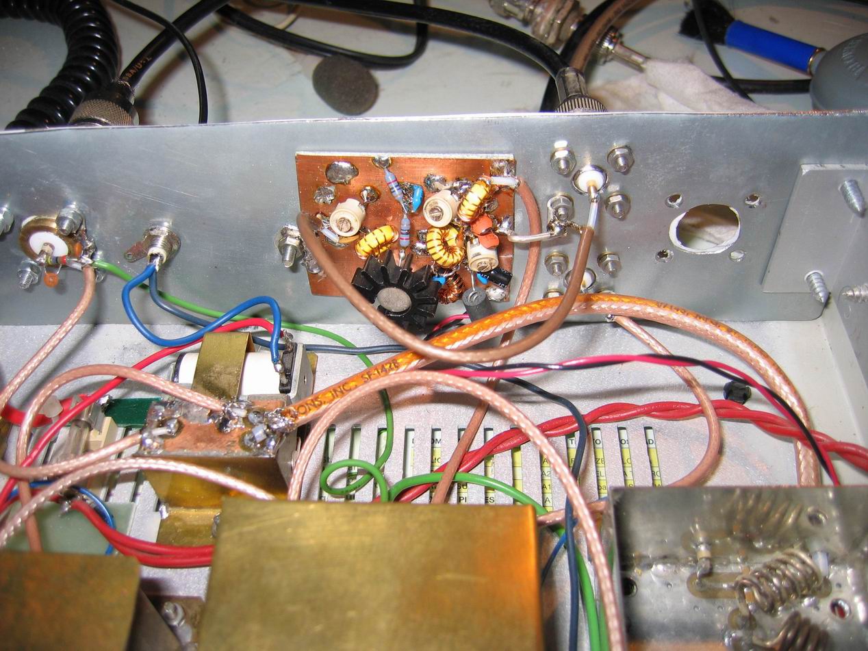
The output signal at 28 MHz from K2 can reach up to 1.27 mW, definitely too low
a level to drive the most transverters. At this point it becomes necessary to
build an amplifier to achieve the necessary level.
I've had built a 13-dB, taken from an old American Handbook, on a piece of pcb
copper mount components in the air (
see photo ).
Overall, the construction of
this switch does not present great difficulties for those who have dexterity
with a soldering iron, perhaps at first glance may seem complicated but well the
project by analyzing one realizes that it is not.
Using
such a system avoids the manual switching of transverters, an operation
increasingly difficult during the band change, even if all we have done and
continue to do so. I hope my idea can help someone or to develop
other ideas here: the fantasy of the Amateur Radio has no limits!
![]()
Fig. 1 - Block Diagram
Fig. 2 - XVOPTO interface schematic
|
|


