
Note: synth kits from both Cumbria Designs and SDR Kits are no longer available. Also the PA module kits from QRPproject! are not available as they have ceased trading.
Design
This transmitter design is based on the control circuitry of the Universal QRP Transmitter which appeared in the April 2006 edition of QST. The case, band pass filters and synthesiser are the same as those used in my Universal Receiver.
The main features of this design are:
| Modular construction giving flexibility for updates |
High frequency stability |
| Adjustable power up to 10 Watts RF output |
Can be built for any, or all, of the current 10 HF bands |
| Rugged PA using easy to build kit, able to withstand high SWR without damage |
Built-in keyer with side tone and memories |
| Vox operation with little shortening of the first "dit" |
Built-in power and SWR metering |
| Compatible with most "boat anchor" receivers as well as more modern ones |
Can use a choice of several synthesizer kits |
| Uses a low pass filter kit to simplify sourcing difficult to find mica capacitors |
Low spurious output, harmonic levels meet FCC requirement |
| Transceives with my Universal Receiver |
|
The final amplifier is the QRP-PA 2008 kit by QRP Project producing up to 10 Watts on all bands. Following the PA is a relay switched low pass filter, the LPF-100 from HF Projects, which is another kit item as I struggled to find suitable capacitors and decided to take the easier option of buying a kit of parts.
The current drawn on standby is approx 350 mA from a 13 Volt supply. On transmit at 10 Watts output the current is 2 ~ 2.5 Amps depending on band.
There is no ALC or high SWR protection, the PA can stand a high SWR and is run well under the maximum rating of the PA transistors.
The transmitter control board improves on the original QST design by shortening the delay between key down and RF appearing, which is now approx 10 mS. The image below shows the letter "i" sent at the beginning of a transmission at roughly 30 WPM, using an external keyer. The K1EL internal keyer can compensate by lengthening the initial character.

Spurious and harmonic outputs are better than -48 dB. See spectrum analyser plots below for each band:
The case used is a "Unicase 2" by Metcase (www.metcase.com), part number M5502119, which measures 260 x 90 x 250mm (W, H, Depth). These cases are stocked in the UK by RS Components (769-4908). An aluminium sheet is fitted in the centre of the case, this is not supplied with the case. I bought a sheet 250mm square by 1mm thick, which is a perfect fit that just needs cutting to length (a sheet thicker than 1mm can be used, but would need to be narrower than 250mm to fit the side channels of the case). At 1mm thick the sheet would normally be considered too thin, however the bandpass filter mother board imparts sufficient stiffness into the sheet. The knobs, including a 31.8mm diameter tuning knob, are from eBay suppliers. The "signal" meter is from Maplin, with illumination by a white LED.
The front panel was produced in Corel Draw and printed on photo card, which in turn was glued to the aluminium panel with photo mount spray adhesive. A clear plastic self adhesive "book protector" film was stuck over the card to protect it.
Some test equipment is essential to the building of this transmitter, the following will be needed:
An L/C meter to measure capacitors and inductors (an LC200A from eBay is adequate and costs around £25), ideally a spectrum analyser with tracking generator, or signal generator and spectrum analyser (or possibly a general coverage receiver if an analyser is not available) to align and check the band pass filters, a power meter and 50 Ohm load, a low cost multi-meter and a frequency counter. An oscilloscope is useful to check the timing of the TX control board but is not strictly necessary. A vector network analyser (VNA) could also be used to align/test the band pass filters. If you are unable to obtain a spectrum analyser, or even a signal generator, it is possible to build the filters and hope they will be OK, however it's a good idea to be able to test each module of the transmitter is working correctly before final assembly.

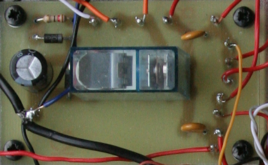
For a view of the underside of the transmitter click here, for an upperside view click here.
Module and circuit details
Below are diagrams in PDF format:
Board layouts in PDF format for etching:
+ Updated Dec 2014 and Feb 2015. Some relays may be polarised, the board layout in version 3 has been changed to facilitate "single side stable" relays. The transistors were drawn reversed in version 2.5, pad size increased in v2.7 resistor RA moved away from TUF-3 in v2.9. Thanks Steve, G4GPY, for spotting this issue.
* Updated Feb 2015, change to reflected power sensitivity (SWR) and capacitor value reduced (Low Power Amp).
There is no PDF layout for the side tone board as being surface mount it is safer to print it directly from the Sprint-Layout file for improved accuracy.
A Zip file of the above boards in Sprint-Layout format can be downloaded here. The viewer version of Sprint-Layout software can be used to print board layouts rather than use the PDF printouts above.
The control board is made using double sided fibreglass board, the upper side is a plain copper earth plane with clearance for non grounded connections obtained by countersink drilling, the other boards are single sided.
The bandpass filter boards are 90 x 25mm single sided, pads are drilled using a 7mm diameter diamond tipped cutter. These are sold for drilling kitchen tiles, members of the GQRP Club can purchase similar pad cutters from the members area of their web site. I do not have a board layout for the keyer, this is a K1EL board and can be obtained from them, or you can use one of their kits which include a PCB.
Power distribution board
The "Off-Stby-Operate-Spot" switch turns on a power relay on the distribution board. An electrolytic capacitor across the relay coil prevents the relay dropping out while rotating the switch between standby, operate and spot. There are two "polyfuse" fuses on the board, check the current needed to supply your synthesiser and uprate the appropriate polyfuse if necessary. 500 mA polyfuses should suffice for most purposes.
The relay was a surplus one I had in my junk box, if your relay has different pin spacing adjust the print layout to suit before etching a board. Note, the print board layout shows several terminal posts for -ve connections, unfortunately my original board only had one.
Control and mixer board

Notice the board shown above is a mirror image of the file for Sprint-Layout
This board is based on the MKII Universal QRP transmitter
by W7ZOI with changes to the keying output to minimise shortening of the initial "dit" at the start of a transmission, C13 partly controls this timing and is reduced from the original 680nF to 330nF. Keying wave shape is mainly controlled on both the leading and trailing edges by the combination of C16, R15 and R19. With the original values the rise time was a little hard, by increasing R19 from 3K3 to 5K6 the wave shape is much better. The rise and fall times of the keyed envelope are 5 mS.
Tr3 switches on the crystal mixing oscillator, holding the supply on for a duration timed by R18 and C12. Tr1 forms a Colpitts oscillator operating at an IF frequency of 8.215 MHz, which is buffered by Tr2 and fed by a low pass filter to a TUF-3 double balanced diode ring mixer. Attenuators formed by RA, RB, RC, RX, RY and RZ reduce the 8.215 MHz and synthesizer levels to feed the TUF-3. It is probably easier to assemble the board minus the TUF-3 mixer, then measure the levels of the crystal oscillator and synthesizer, adjusting the attenuators if necessary.
The output from the mixer needs to be around -16 dBm. An output spectrum analyser plot of the mixer output is shown below, this is a direct feed to the analyser from the TUF-3. The synthesizer is operating with an output around 15 MHz with a wanted frequency of 7 MHz, the image frequency is 23 MHz. The wanted signal and image are both at -14 dBm, immediately to the right of the 7 MHz signal is the 8.215 MHz IF leakage at -56 dBm and mid way between the two -14 dBm signals is the synthesizer leakage at -58 dBm.

C15 and R24 give a hold time sufficient for semi break-in keying, a value of 16uF for C15 is suitable for keying speeds of 18 ~ 25 WPM, rising to 22uF for slower hand keying. A 16 uF capacitor will give a hold time of approximately 350 mS. The actual value is a matter of personal preference.
It is important to use a high speed relay otherwise there is a risk of hot switching the PA, with the values shown the time between the collector of Tr9 going low and RF appearing is 10mS. The Panasonic relay specified has a change over time of 4mS. One pair of relay contacts change over the antenna and the other pair mute the receiver by open circuiting a ground connection, this method of receiver muting is used by my Univeral Receiver and many boat anchor receivers. Beware that some of these relays are polarised, which means the relay will only operate with the correct polarity on the coil.
Diode D5 has been added to provide linear keying for a modern linear with fast change over and low keying Voltage/current. It works fine with an Elecraft KPA500 which has QSK and diode antenna change over. It is not a suitable means of keying older and more basic linear amplifiers. There is no additional hold time for a slow switching linear amp. The current drawn by the bias circuit of the PA in my transmitter is 17 mA, if you intend to use a different PA which may draw higher current, Tr8 may need to be a higher current device. The existing 2N3906 is rated at 200 mA of continuous collector current.
The original standby/operate switching has been modified, now on standby the link between R19 and the key(er)/ tune switch is broken by switch contacts S1c. This allows the side tone to operate while in standby, as well as in operate.
The image below shows the various timing and output levels. Yellow (trace #1) is internal keyer output, magenta (trace #3) is the RF output at the antenna socket, cyan (trace #2) is the mute line output and dark blue (trace #4) is the oscillator supply. Note the internal keyer has compensation to lengthen the initial character.

The image below shows a close up of the relationship between the key line going low (yellow trace #1) and the mute output going high (cyan trace #2). The RF output from the antenna socket is shown in magenta (trace #3). The relay contacts open in less than 3 mS, assuming the RF change over contacts operate at the same time there is easily enough time for the relay to operate before RF is generated. Another Panasonic relay was measured in a Universal QRP transmitter with similar timing.

Synthesiser
I used a standard kit from Cumbria Designs, however these may have been discontinued. There are several similar synthesiser kits around which are suitable, the requirement being an output level of 7 ~ 10 dBm and a frequency range of 10 ~ 40 MHz. SDR Kits produce a suitable unit which also includes automatic band switching for filters. The Cumbria synthesiser is based on an Si570 device outputting +10 dBm into 50 Ohm and is used with a Bourns 64 pulse per revolution optical shaft encoder in place of the supplied mechanical encoder. The encoder push switch is used as a "tune" switch, wired across the key input, although a separate button could be added to the front panel. The"F/S" (fast/slow/variable tuning speed) button is wired in place of the one originally used with the encoder switch.
Once left on a frequency for around one minute, the frequency is internally stored in the synthesiser allowing the transmitter to be powered up on the last used frequency. This feature may not be available with other synthesiser kits.
Frequency stability is far better than the specification of the Si570 suggests. Frequency drift after a couple of minutes warm up was 30 Hz in the first half hour, followed by virtually no drift afterwards, or at least only 1 Hz or so. This was measured in a centrally heated shack at the final transmitted output frequency on the 10 metre band, using a Racal 9916 counter which was locked on frequency with a GPS derived standard. I didn't try the effect of cooling or heating.
Optional switching between the internal synthesiser and an external one in the Companion Receiver is accomplished with a double pole change over relay mounted on the control board and switched using a front panel mounted toggle switch. The un-used synthsiser (or buffer) output is terminated in a 50 Ohm resistor to minimise stray RF. The control board layout has not been updated to accommodate the additional relay. The image below shows the relay in the bottom right corner, note the cross connections on the relay.

Band Pass Filters

There are 10 band pass filter boards selected by a 1 pole 12 way front panel switch. Each board is constructed on single sided PCB to avoid possible shorts between adjacent boards. Each filter was individually tested/aligned before being added to the main board. The filter design is the same as used in my Universal Receiver and was done using the freeware Windows program "Elsie", using a topology of "Mesh Capacitor-coupled band pass" and "Chebyshev" Family of 3rd order (uses 3 inductors and 5 capacitors per filter, actually produces "5th order filter"). The design was altered to use the nearest 5% capacitor value with inductors wound for the required inductance using a low cost L/C meter. For those not familiar with this program, beware of the default Q settings of capacitors and inductors being excessive (a value of 200 ~ 500 is more realistic) and also set the transmission to "Absolute", both these settings are found under the "Analysis" tab.
The narrower the bandwidth of a filter, the greater the loss through it. As the Elsie program is so easy to use, it's worth experimenting with bandwidth to make the filters less critical to set up, and perhaps to see if you can use near value capacitors when sourcing the exact value is proving difficult. I don't think it's worth trying to source silver mica or polystyrene capacitors, they can be expensive and hard to find. I mostly used ordinary ceramic capacitors and film trimmers for the higher bands. The image below is a spectrum analyser plot of the response of the 14 MHz band pass filter, measured between the in/out buss bars. The loss is 3dB. 
While it's not strictly necessary to use such elaborate filters in a transmitter, the virtually total elimination of image and other spurious frequencies is worth the small additional cost and effort. Purists may wish to add an attenuator to the output of some filters in order to match the loss across all the filters. Typically the loss will vary from around 1 ~ 3 dB for each filter when measured through the relays and buss bar connections. Up to 4dB loss can be accommodated by the gain of the low power amplifier.
Capacitor and inductor values are critical, being off by a few percent can make a huge difference to performance. Unless you can source close tolerance capacitors, you will generally have to make up the required values by connecting 2 or 3 in parallel and measuring the value with an LC meter. The toroids should be wound for an extra turn and then fine adjusted by removing a turn or two and/or moving the wires on the core until you obtain the required value, estimating the value based on the number of turns may not produce good results. The ideal way to measure the inductance is to check the resonant frequency with a known value capacitor in parallel using a dip meter. Unfortunately, many of the LC meters use a 500 KHz oscillator and this can lead to problems with coils wound on iron dust cores, such as the ones used in these band pass filters. For the higher bands, trimmers were used for the series capacitors (7 MHz and above). T50-2 cores were used from 1.8 to 10 MHz with T50-6 on the higher bands.
The switching relays are generic double pole change over signal relays with 12 Volt coils, a 1N4148 diode is wired across the coil to stop back EMF when switching and each DC switching line is de-coupled to the ground plane of the band pass board. Beware that some relays can have polarised coils, which means they will not operate with reversed polarity... Check before soldering!
Each band pass filter is "tack" soldered to a mother board, with the relay switched input/output soldered to a common bus bar. Note the low pass filters I used have polarised relays which require a permanent +ve supply, which is grounded through the relay, this differs from the switching arrangement used in the Universal Receiver.
Low Power Amplifier

This amplifier is based on a design in Experimental Methods in RF Design, by the ARRL. The original design had a far from flat frequency response curve and was a poor match to the 50 Ohm band pass filters. By careful tweaking of the components of the first stage, the amplifier can give a response which is flat to within 1 dB from 1 MHz to 30 MHz. The gain ranges from approx 20 to 30 dB depending on the setting of the power control, that includes the loss through the 3dB output attenuator. The 1N4007 behaves as a PIN diode in this circuit allowing for gain adjustment between typically 2 and 10 Watts from the PA (the lower power level depends on the band pass filter loss). The image above shows a second board assembled and tested prior to fitting in a transmitter. The 3 dB output attenuator resistors are mounted under the board. Click here for an image of the spectrum sweep of the above board, note the spectrum analyser has a 20 dB external attenuator fitted. The input to the board is -20 dBm, the output approx +12 dBm. The "wobble" on the trace in the region of 2 ~ 3 MHz is an artefact of the analyser and it's connections, not the low power amp.
The 100nF capacitor that was in series with the 1N4007 diode has been reduced to 10nF, this is to remove a momentary spike in power level that occurred at the leading edge of each character when the power level was set around 75% of full power.
If you are struggling for power on higher frequencies when using this amplifier board, do not increase the value of C1 beyond about 220 pF. Too much capacitance between the emitter of the BSX20 and the 1N4007 will create a spike at the leading edge of the transmit envelope due to momentarily increasing the Voltage on the anode of the diode. The better solution is to add a capacitor of between 1nF and 4.7nF across the 4.7 Ohm resistor on the emitter of the 2N3866. Also, do not remove the output attenuator as this provides a better match between the low power amplifier and the following PA amplifier.
Power Amplifier
This is an easy to build kit from Germany which gives a flat response from 1.8 to 30 MHz, dropping to 3dB down at 50 MHz. The output is 10 Watts and can withstand a high SWR without needing ALC protection. Following investigation for lower than expected output power on some bands, a sweep of the combined low power amplifier and the PA showed an unexpected peak in the 32 MHz region, adding a 3 dB attenuator to the output of the low power amplifier cured this instability.
The transistors are bolted to an aluminium heatsink approximately 111mm wide x 60mm high and 25mm deep.
Low Pass Filter
Having struggled to source capacitors, I took the easy route and bought a kit from HF Projects in the USA. Update: Try Rapid in the UK for silver mica caps! There is nothing special about the low pass filter requirement for this transmitter and any similar design could be used. I consider the attenuation of the 2nd harmonic on 1.8 MHz (3.6 MHz) and also the 2nd harmonic of 5.3 (10.6 Mhz) to be marginal at roughly 48 ~ 52dB below peak output, however, the FCC requirement for harmonic attenuation is 40 dB, or better, for 10 Watt transmitters and this filter meets that. The Cauer filter used on 40m/60m is very effective when used on 40m but the notches are not effective against the harmonics on 60m. Better filters can be designed using Elsie, and if you opt for an extra low pass filter for the 60m band, the overall performance with regard to harmonics can be improved. However, obtaining the required capacitor values can be difficult and the overall harmonic output is lower than some commercial kit transceivers that run higher power.
Keyer
The keyer board uses a K14 PIC by K1EL and provides an internal keyer with memories. I bought the IC and made a copy of the keyer board in order to keep the cost under the UK import limit for charging VAT and handling, however a complete kit, including PCB is available from K1EL. The side tone from the keyer board is fed via a rear panel toggle switch to an internal speaker for local copy and programming/set up, which can be used for practice or if used with a receiver that doesn't include side tone input. Note... in order to program the K14 keyer you need a local speaker as the output for a TX is not enabled when programming the memories, etc.
I added an extra 7mS to the initial character in order to avoid character shortening in this transmitter, there is a parameter in the K1EL keyer to accommodate this (extended command "E"). On another transmitter the character shortening was the same, but on a third the shortening was found to be 12 mS, which was easily compensated for. The reason for the difference was not investigated.
Side Tone
Since originally building the transmitter, the lack of a side tone for the hand key input became annoying. Adding side tone is fairly straightforward, although building one that doesn't click and thump as it's keyed required a little experimentation. Eventually I settled on a design from the ARRL book "Experimental Methods in RF Design", it is shown on page 6.40 of that book and is reproduced with permission in the diagrams further up the page. The output is a 750 Hz sinewave, although the frequency will vary slightly depending on the tolerance of the 10 nF capacitors and the 22K resistors.
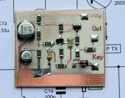
Not having 5.1K resistors in my parts box, I substituted 4.7K instead, only to find the oscillator reluctant to start. Reducing R9 to 3.9K cured the problem. The side tone works well from below 9 Volts up to 15 Volts with these values. Note the control board has been modified to use a different method of standby/operate switching in order to use this side tone.
The board was made using 1206 size SMD parts, except for D1 as I didn't have a suitable SMD diode. The board layout is intended to be used with an SMD diode. I soldered the edge of the board to my keyer board, however it can be "tagged" to any board where there is space, or even screwed down. SWR and Power Board

The output of an SWR and Power measuring bridge is amplified with a CA3130 operational amplifier. The meter output is fed via D5 and D6 to improve the linearity. My meter is a basic "signal" meter marked 1 to 5, which corresponds to half the measured output power. The meter reads the peak RF level, holding the reading for several milliseconds by the charge held by C19. C12 is adjusted for minimum reflected power when terminated with a 50 Ohm dummy load. R28 can be reduced slightly if you cannot obtain full scale with 10 Watts output. R23 and R24 set the forward and reflected levels.
Since originally building the transmitter, the poor SWR measurement concerned me. Forward power measurement was good, so I took the solution to switch out diodes D5 and D6 on reflected, which can easily be done by using a double pole toggle switch and bypassing the diodes when switched to read reflected power. I am able to obtain 5 and 10 Watts forward to read 2.5 and 5 on the 0 - 5 meter scale, and 2:1 and 3:1 SWR (at 10 Watts) on the "2" and "3" marks on the meter. The readings are approximate, but good enough for most purposes.
Note the missing meter diodes and input zener in the above image.
In common with other builders of SWR meters like this one, if you find the forward and reflected readings are reversed, just swap the wires.
Construction tips
This transmitter was built as a one off, with circuits and print board layouts to help anyone else who wishes to use them. As such it isn't intended to be a "Heathkit" project where you slavishly follow the diagrams, switch on and find it works! Most of the boards can, and should, be assembled and tested before wiring them together. The critical points to watch for are:
1. While I have taken care to check the board layouts are correct, please double check them yourself before etching. Some of the print board pads are quite small, feel free to increase their size if your drilling and soldering is a bit shakey. The board layouts are intended for home printing/etching, I have no idea if they are suitable for commercial board suppliers. Likewise the circuit diagrams are believed to be OK. If you have any questions I am only an e-mail away, however, this is a "do it yourself" project for experienced constructors and as such I can only offer limited support. 2. The output of the mixer, and the loss through the bandpass filters, are matched to the gain of the low power amplifier. If you cannot obtain -16 dBm from the mixer and less than 4 dB loss through the filters, the output will be low.
3. Inductors wound on iron dust toroid cores can be tricky to measure, the problem is that most common LC meters use an oscillator around 500 KHz and that is very low compared to HF frequencies which can result in significant errors - especially on the higher frequencies using T50-6 cores. However, inductor values are easy to measure in the old manner of using a known value capacitor of good accuracy, such as a 1% silver mica one, then tagging the capacitor in parallel with the inductor and measuring the resonant frequency with a dip meter, it's then an easy matter of calculating the inductor value or using one of the on-line calculators. If the test capacitor is chosen to resonate the inductor near the planned frequency, then the results should be close to ideal.
4. Some components are becoming hard to source. Currently the TUF-3 can be obtained from Cumbria Designs. The synthesizer I used is no longer offered by Cumbia, although SDR-Kits have a suitable alternative. Toroids can be obtained at a good price from the G-QRP Club (members only). Capacitors for the bandpass filters can sometimes be found on eBay, although their quality and tolerance can be quite variable. Recently Rapid in the UK have good stock of silver mica capacitors which are only specified as being 5% but were measured at around 1%. The heatsink and wire for the transformers and coils can also be found on eBay.
5. While I built a 10 band transmitter, in reality it spends most of it's time on 40m and 80m. Occasionally I also use it on 20m. A three band transmitter would have been quicker to build and could be expanded to more bands later if necessary. Making a low pass filter board for 3 bands means you have space to build very effective Cauer filters with a steep drop off to the high frequency side of the transmit frequency, sourcing capacitors for 3 bands is much easier than for 10 bands too.
6. Either having a spectrum analyzer, or the loan of one from a fellow ham, makes alignment very simple. The relatively low cost Rigol DSA 815 TG was used in the contruction of this transmitter.
Alignment
The output of the synthesizer and crystal oscillator were checked and the attenuator values adjusted to obtain +7 dBm and -10 dBm respectively before fitting the TUF-3 on the control board. The output of the control board should then be -16 dBm for the wanted and image frequencies.
Each band pass filter board was tested/aligned before adding them to the mother board. Those with trimmer capacitors were adjusted for maximum signal towards the middle part of the CW portion of each band, there was no need to stagger tune them. A final adjustment for maximum power can be done with the boards soldered in place. A spectrum analyser with tracking generator was used for alignment.
The PA bias was set as per the kit instructions and the output checked with a signal generator providing the +10 dBm drive. Beware you need a heatsink on the PA transistors, even when setting the bias.
If built as a stand alone transmitter, the 8.215 MHz crystal trimmer should be set to 8.215 MHz using a frequency counter connected to the output of the low pass filter, the synthesiser should be similarly adjusted to give the calculated injection frequency on the 29 MHz band (indicated frequency plus 8.215). A final check was conducted at 29 MHz to ensure the dial correctly read the frequency.
If the transmitter is intended to be used to transceive with the Universal Receiver, the crystal trimmer on the control board has to be set to match the receiver's synthesiser. In the case of using the external synthesiser from the Universal Receiver, the alignment sequence is as follows: 1. Allow both the transmitter and receiver 30 minutes of warm up time and select 28 or 29 MHz on both. Set the receiver synthesiser/display/BFO correctly first, in particular check that a signal on the indicated dial frequency on CW gives exactly a 750 Hz output tone. Use either an accurate signal generator or crystal marker. The easiest way to check the setting of the receiver is with a "smart phone" or tablet computer running one of the many audio spectrum or musical instrument tuning apps. On SSB tune 1 KHz off frequency and check for a 1000 Hz tone, on CW tune to the frequency and check for a 750 Hz tone.
2. Select external synthesiser input and transmit, adjust the 8.215 MHz crystal on the control board to give the same transmit frequency as indicated on the receiver display.
3. Switch back to use the transmitter internal synthesiser, the transmit frequency will be off by a few hundred Hz. Adjust the transmitter synthesiser offset to give the correct transmit frequency.
4. Switch back and forth between internal and external synthesisers to ensure there is no difference in transmit frequency or dial frequency. Check the other bands also give the correct frequencies.
Conclusion
The transmitter works remarkably well and receives excellent reports. The keying and side tone work smoothly with no clicks or thumps.
The circuit diagrams and board layouts were drawn using sPlan 7 and Sprint-Layout 6 from Abacom. Click here for a link to their site.
Elsie can be downloaded from here.
K1QW has a useful calculator for toroid inductors, it can be downloaded here.
K1EL, the keyer board, is here
The source of the PA board is here
And SDR-Kits are here
Please do not build this design without checking the values for yourself, in particular the band pass filter components. The information is presented here to assist experienced constructors who may wish to build something similar, it is not suitable for novice constructors.


|
