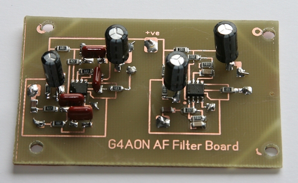
A peak audio filter centered around 750 Hz is commonly added to many home built receivers and transceivers. My Universal Receiver only had a low pass audio filter, so I added a peak filter for CW. Not having room to fit a second board, I designed a board using surface mount components to fit in place of the existing pre-amp/low pass filter board. I've produced two versions of the board, a simpler one, version 2, which is shown above and a slightly more complex one, version 3, shown below.
Both boards have identical 750 Hz peak filters on the left hand side. The version 2 board has a simple low pass filter which has a peak response around
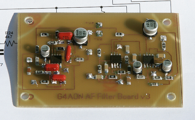
1 KHz. The version 3 board has more effective filtering followed by an op amp to match the gain to that of the peak filter. In addition I've used SMD electrolytic capacitors in the later version. However, either board can be built using conventional "through hole" components if you design a suitable board. These boards were intended to fit an existing space in my Universal Receiver and also doubled as SMD construction experiments.
Version 2, circuit description
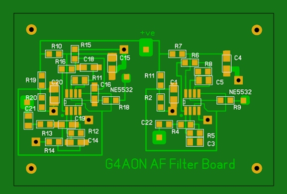
Click here for a PDF file of the circuit diagram. The filter board comprises two separate circuits, one half is a 2 section band pass filter with a peak at 750 Hz and the other, a low pass filter. The circuitry is standard, the low pass filter is reproduced with permission from the ARRL publication "Experimental Methods in RF Design", page 640.
1206 sized SMD capacitors and resistors are used. Oversize pads have been drawn to accommodate larger capacitors at C1, 4, 14,15, 16, 18, 19 and 20. If you have 27nF SMD capacitors these could be used instead and will still fit the board.
R18 was chosen to balance the audio level between the peak and low pass filters into a 10K load, in my case the AF gain control. The sidetone input has been moved to the AF gain control in my receiver. If using this board with a different impedance load, adjustments may be necessary to the value of R18.
The input to each filter could be switched, however it was not found necessary.
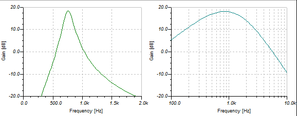
The above image shows the response of the version 2 filter. The peak filter on the left and the low pass filter on the right, as plotted by the circuit simulation software "Tina". Note the frequency scales differ between the plots and the rather poor response curve of the low pass filter with a peak in the 700 Hz to 1 KHz region. However, to be fair to the original design, it does sound fine on SSB and is acceptable for communications purposes.
Construction of the version 2 board
The board design was done with Sprint-Layout from Abacom, click here to visit their site. A zip file of the board layout file is here. There is a viewer version of Sprint-Layout on the Abacom site that can be used to print the board if you do not have their full version. Due to the close spacing of the tracks, I have not included a PDF board layout as a print from it is unlikely to be as sharp as a directly printed one from Sprint-Layout.
The tracks were printed as a mirror image onto paper using a laser printer, the tracks were then transferred to the double sided copper board with a clothes iron. The underside of the board was protected with self adhesive "book covering" film before being etched in ferric chloride. There are many YouTube videos showing this simple and cheap technique, so I won't go into details here.
The electrolytic decoupling capacitors and 27nF filter capacitors are conventional "through hole" components mounted on the top side of the board. The underside of the PC board is a plain copper earth plane to facilitate easy construction and ground connections. There are 7 holes needed to link the top side of the board with the ground plane underneath, these are shown as square pads with black holes in the board layout above. The four corner mounting holes are isolated from ground by cuts in the copper ground plane, this helps avoid ground loops.
The first stage of soldering is to apply solder paste to all the SMD pads, dropping each component into location in turn. I used a cheap Chinese hot air soldering station with a 6mm nozzle to solder the SMD parts on the board, then added the wired capacitors using a conventional soldering iron.
The board was tested on the bench prior to adding to my receiver. The peak filter response was 6 dB down at 663 and 854 Hz, giving a bandwidth of 183 Hz. The filter doesn't have cliff edge sides to it's response, as it's only a two stage analogue filter, but it does dramatically reduce background noise making CW reception very smooth.
Version 3, circuit description
Click here for a PDF file of the circuit diagram. The 750 Hz CW peak filter, U1 and associated components, is identical to that in the version 2 design. I used the same "through hole" wire ended capacitors for the filter capacitors (C14, 16, 18 and 19). If you have suitable SMD capacitors, these could be used instead. R18 matches the output level to that of the low pass filter section.
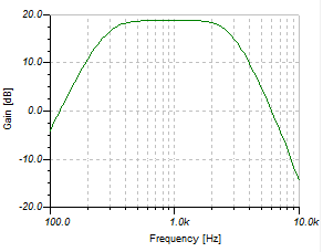
The above image shows the much improved response of the version 3 low pass filter, compare the graph with that of the simpler version 2 board.
Actually the input to the low pass filter comprises an input high pass filter to restrict the unwanted audio below 300 Hz, followed by both passive and active low pass filtering in U2b to roll off frequencies above 3 KHz. The gain across U2a/U2b is approximately unity. U3 amplifies the output of U2b to match the output of the 750 Hz peak filter, U1a/U1b. Component values are fairly critical in this filter, note the Voltage divider, R2/R11 uses 5K6 resistors, this is to work in conjunction with C28 and forms part of the filter. R27 and R28 are chosen to provide a slightly lower Voltage on the -ve side of C25 in order to avoid possible reverse bias on it. C23 would normally be 22 pF in HiFi applications, by using a larger value of 3n3 there is additional attenuation of the higher frequencies, typically a further 4 or 5dB at 10 KHz. A larger value than 3n3 at C23 causes excessive roll off around the 3 KHz region. Note that pin 1 of U3 is not connected.
Thanks to Dave, GM4EVS, for his assistance with the design of the low pass filter.
Construction of the version 3 board
The version 3 board is no harder to assemble than the version 2 board. Be careful with component placement as the low pass filter half of the board has closer spaced parts in order to fit a third op amp onto the board. 1206 sized components are used throughout, although in some places 0805 sized parts can be used. Beware of the tracks passing under R25, R27, etc. As per the version 2 board, I used double sided board with a plain copper ground underneath, the 9 square pads are for through connections to provide -ve connections. Cut the underside copper to isolate the mounting holes to avoid earth loops.
Click here for a Zip file of the version 3 board in Sprint Layout format. As per the version 2 board, I have not included a PDF board layout as the printing needs to be sharp and accurate. 

|
